 | –≠–ª–µ–∫—Ç—Ä–æ–Ω–Ω—ã–π –∫–æ–º–ø–æ–Ω–µ–Ω—Ç: 24C21 | –°–∫–∞—á–∞—Ç—å:  PDF PDF  ZIP ZIP |
1
Features
∑
2-Wire Serial Interface
∑
Schmitt Trigger, Filtered Inputs For Noise Suppression
∑
DDC1TM/ DDC2TM Interface Compliant for Monitor Identification
∑
Low Voltage Operation
≠ 2.5 (V
CC
= 2.5V to 5.5V)
∑
Internally Organized 128 x 8
∑
100 kHz (2.5V) Compatibility
∑
8-Byte Page Write Mode
∑
Write Protection Available
∑
Self-timed Write Cycle (10 ms max)
∑
High Reliability
≠ Endurance: 1 Million Write Cycles
≠ Data Retention: 100 Years
≠ ESD Protection: >3000V
∑
8-Pin PDIP and JEDEC SOIC Packages
Description
The AT24C21 provides 1024 bits of serial electrically erasable and programmable
read only memory (EEPROM) organized as 128 words of 8 bits each. The device is
optimized for use in applications requiring data storage and serial transmission of con-
figuration and control information. The AT24C21 features two modes of operation:
Transmit-Only Mode and Bidirectional Mode. Upon power-up, the AT24C21 will be in
the Transmit-Only Mode, sending a serial-bit stream of the entire memory contents,
clocked via the VCLK pin. The Bidirectional Mode is selected by a valid high-to-low
transition on the SCL pin and offers byte selectable read/write capability of the entire
memory array. The AT24C21 is available in space saving 8-pin PDIP and 8-pin SOIC
packages.
2-Wire Serial
EEPROM
1K (128 x 8)
AT24C21
Rev. 0405E≠07/98
2-Wire, 1K
Serial EEPROM
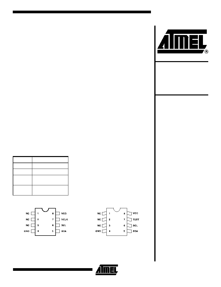
Pin Configurations
Pin Name
Function
NC
No Connect
SDA
Serial Data
SCL
Serial Clock Input
(Bidirectional Mode)
VCLK
Serial Clock Input
(Transmit-Only Mode)
8-Pin PDIP
8-Pin SOIC

AT24C21
2
Block Diagram
Pin Description
SERIAL CLOCK (SCL): The SCL input is used to positive
edge clock data into each EEPROM device and negative
edge clock data out of each device.
SERIAL DATA (SDA): The SDA pin is bidirectional for
serial data transfer. This pin is open-drain driven and may
be wire-ORed with any number of other open drain or open
collector devices.
SERIAL CLOCK (VCLK): Upon power-up, the device is in
the Transmit-Only mode and will transmit the entire mem-
ory contents via the SDA pin with positive signals on the
VCLK pin.
Memory Organization
AT24C21, 1K SERIAL EEPROM: Internally organized with
128 pages of one byte each. The 1K requires a 7-bit data
word address for random word addressing.
Absolute Maximum Ratings*
Operating Temperature ................................. -55
∞
C to +125
∞
C
*NOTICE:
Stresses beyond those listed under "Absolute
Maximum Ratings" may cause permanent dam-
age to the device. This is a stress rating only and
functional operation of the device at these or any
other conditions beyond those indicated in the
operational sections of this specification is not
implied. Exposure to absolute maximum rating
conditions for extended periods may affect device
reliability.
Storage Temperature .................................... -65
∞
C to +150
∞
C
Voltage on Any Pin
with Respect to Ground .....................................-1.0V to +7.0V
Maximum Operating Voltage........................................... 6.25V
DC Output Current........................................................ 5.0 mA

AT24C21
3
Note:
1. V
IL
min and V
IH
max are for reference only and not tested.
Note:
1. This parameter is characterized and is not 100% tested.
DC Characteristics
Applicable over recommended operating range from: T
AI
= -40
∞
C to +85
∞
C, T
AC
= 0
∞
C to +70
∞
C, V
CC
= +2.5V to +5.5V
(unless otherwise noted).
Symbol
Parameter
Test Condition
Min
Typ
Max
Units
V
CC
Supply Voltage
2.5
5.5
V
I
CC
Supply Current V
CC
= 5.0V
READ at 100 KHz
0.4
1.0
mA
I
CC
Supply Current V
CC
= 5.0V
WRITE at 100 KHz
2.0
3.0
mA
I
SB
Standby Current .......V
CC
= 2.5V
.......V
CC
= 5.0V
V
IN
= V
CC
or V
SS
V
IN
= V
CC
or V
SS
3.0
12.0
4.0
30.0
µ
A
µ
A
I
LI
Input Leakage Current
V
IN
= V
CC
or V
SS
0.10
1.0
µ
A
I
LO
Output Leakage Current
V
OUT
= V
CC
or V
SS
0.05
1.0
µ
A
V
IL
Input Low Level
(1)
SCL, SDA Pin
Input Low Level VCLK Pin
V
CC
2.7V
V
CC
< 2.7V
-0.6
V
CC
◊
0.3
0.8
0.2
◊
V
CC
V
V
V
V
IH
Input High Level
(1)
SCL, SDA Pin
Input High Level VCLK Pin
V
CC
◊
0.7
2.0
V
CC
+ 0.5
V
V
V
OL
Output Low Level V
CC
= 3.0V
I
OL
= 2.1 mA
0.40
V
Pin Capacitance
(1)
Applicable over recommended operating range from T
A
= 25
∞
C, f = 1.0 MHz, V
CC
= +1.8V.
Symbol
Test Condition
Max
Units
Conditions
C
I/O
Input/Output Capacitance (SDA)
8
pF
V
I/O
= 0V
C
IN
Input Capacitance (A
0
, A
1
, A
2
, SCL, VCLK)
6
pF
V
IN
= 0V
Transmit-Only Mode
Symbol
Parameter
2.5-volt
Units
Min
Max
T
VAA
Output valid from VCLK
500
ns
T
VHIGH
VCLK high-time
4.0
µ
s
T
VLOW
VCLK low-time
4.7
µ
s
T
VHZ
Mode transition time
500
ns
T
VPU
Transmit-Only power-up time
0
ns

AT24C21
4
Note:
1. This parameter is characterized and is not 100% tested.
AC Characteristics
Applicable over recommended operating range from T
A
= -40
∞
C to +85
∞
C, V
CC
= +2.5V to +5.5V C
L
= 1 TTL Gate and
100 pF (unless otherwise noted).
Symbol
Parameter
2.5-volt
Units
Min
Max
f
SCL
Clock Frequency, SCL
0
100
KHz
t
LOW
Clock Pulse Width Low
4.7
µ
s
t
HIGH
Clock Pulse Width High
4.0
µ
s
t
I
Noise Suppression Time
(1)
(SDA and SCL pins)
NA
ns
t
AA
Clock Low to Data Out Valid
0.1
3.5
µ
s
t
BUF
Time the bus must be free before a new
transmission can start
4.7
µ
s
t
HD.STA
Start Hold Time
4.0
µ
s
t
SU.STA
Start Set-up Time
4.7
µ
s
t
HD.DAT
Data In Hold Time
0
µ
s
t
SU.DAT
Data In Set-up Time
250
ns
t
R
Inputs Rise Time
(1)
1.0
µ
s
t
F
Inputs Fall Time
(1)
300
ns
t
SU.STO
Stop Set-up Time
4.0
µ
s
t
DH
Data Out Hold Time
100
ns
t
WR
Write Cycle Time
10
ms
Endurance
(1)
5.0V, 25∞C, Page Mode
1M
Write Cycles

AT24C21
5
Functional Description
The AT24C21 has two modes of operation: the Transmit-
Only Mode and the Bidirectional Mode. There is a separate
2-wire protocol to support each mode, each having a sepa-
rate clock input (SCL and VCLK) and both modes sharing a
common Bidirectional data line (SDA). The AT24C21
enters the Transmit-Only Mode upon powering up the
device. In this mode, the device transmits data on the SDA
pin upon a clock signal on the VCLK pin. The device will
remain in the Transmit-Only Mode until a valid high-to-low
transition takes place on the SCL pin. The device will
switch into the Bidirectional Mode when a valid transition
on the SCL pin is recognized. Once the device has transi-
tioned to the Bidirectional Mode, there is no way to return to
the Transmit-Only Mode, except to power down (reset) the
device.
Transmit-Only Mode (DDC1)
The AT24C21 will power up in the Transmit-Only Mode. In
this mode, the device will output one bit of data on the SDA
pin on each rising edge on the VCLK pin. Data is transmit-
ted in 8 bit words with the most significant bit first. Each
word is followed by a 9th "don't care" bit which will be in
high impedance state (refer to Figure 1). The AT24C21 will
continuously cycle through the entire memory array in
incremental sequence as long a VCLK is present and no
falling edges on SCL are received. When the maximum
address (7FH) is reached, the output will wrap around to
the zero location (00H) and continue. The Bidirectional
mode clock (SCL) pin must be held high for the device to
remain in the Transmit-Only mode.
Upon power-up, the AT24C21 will not output valid data until
it has been initialized. During initialization, data will not be
available until after the first nine clocks are sent to the
device (refer to Figure 2). The starting address for the
Transmit-Only mode can be determined during initializa-
tion. If the SDA pin is held high during the first eight clocks
(refer to Figure 2), the starting address will be 7FH. If the
SDA pin is low during the first eight clocks, the starting
address will be 00H. During the ninth clock, SDA should be
in high impedance.
Figure 1. Transmit-Only Mode
Figure 2. Device Initialization for Transmit-Only Mode