
Rev. 4118H≠AERO≠06/03
F
eatures
∑
Integer Unit Based on SPARC V7 High-performance RISC Architecture
∑
Optimized Integrated 32/64-bit Floating-point Unit
∑
On-chip Peripherals
≠ EDAC and Parity Generator and Checker
≠ Memory Interface
Chip Select Generator
Waitstate Generation
Memory Protection
≠ DMA Arbiter
≠ Timers
General Purpose Timer (GPT)
Real-time Clock Timer (RTCT)
Watchdog Timer (WDT)
≠ Interrupt Controller with 5 External Inputs
≠ General Purpose Interface (GPI)
≠ Dual UART
∑
Speed Optimized Code RAM Interface
8- or 40-bit boot-PROM (Flash) Interface
∑
IEEE 1149.1 Test Access Port (TAP) for Debugging and Test Purposes
∑
Fully Static Design
∑
Performance: 12 MIPs/3 MFlops (Double Precision) at SYSCLK = 15 MHz
∑
Core Consumption: 1.0W Typ. at 20 MIPs/0.7W typ. at 10 MIPs
∑
Operating Range: 4.5V to 5.5V
(1)
-55
∞
C to +125
∞
C
∑
Total Dose Radiation Capability (Parametric and Functional):
300 KRADs (Si)
∑
SEU Event Rate Better than 3 E-8 Error/Component/Day (Worst Case)
∑
Latch-up Immunity Better than (LET) 100 MeV-cm
2
/mg
∑
Quality Grades: ESA SCC, QML Q or V
∑
Package: 256 MQFPF; Bare Die
Note:
1. For 3.3V capability see the TSC695FL datasheet on the Atmel site.
Description
The TSC695F (ERC32 Single-Chip) is a highly integrated, high-performance 32-bit
RISC embedded processor implementing the SPARC architecture V7 specification. It
has been developed with the support of the ESA (European Space Agency), and
offers a full development environment for embedded space applications.
The processor is manufactured using the Atmel 0.5 µm radiation tolerant (
300
KRADs
(Si)) CMOS enhanced process (RTP). It has been specially designed for
space, as it has on-chip concurrent transient and permanent error detection.
The TSC695F includes an on-chip Integer Unit (IU), a Floating Point Unit (FPU), a
Memory Controller and a DMA arbiter. For real-time applications, the TSC695F offers
a high security watchdog, two timers, an interrupt controller, parallel and serial inter-
faces. Fault tolerance is supported using parity on internal/external buses and an
EDAC on the external data bus. The design is highly testable with the support of an
On-Chip Debugger (OCD), and a boundary scan through JTAG interface.
Rad-Hard 32-bit
SPARC
Embedded
Processor
TSC695F
2
TSC695F
4118H≠AERO≠06/03
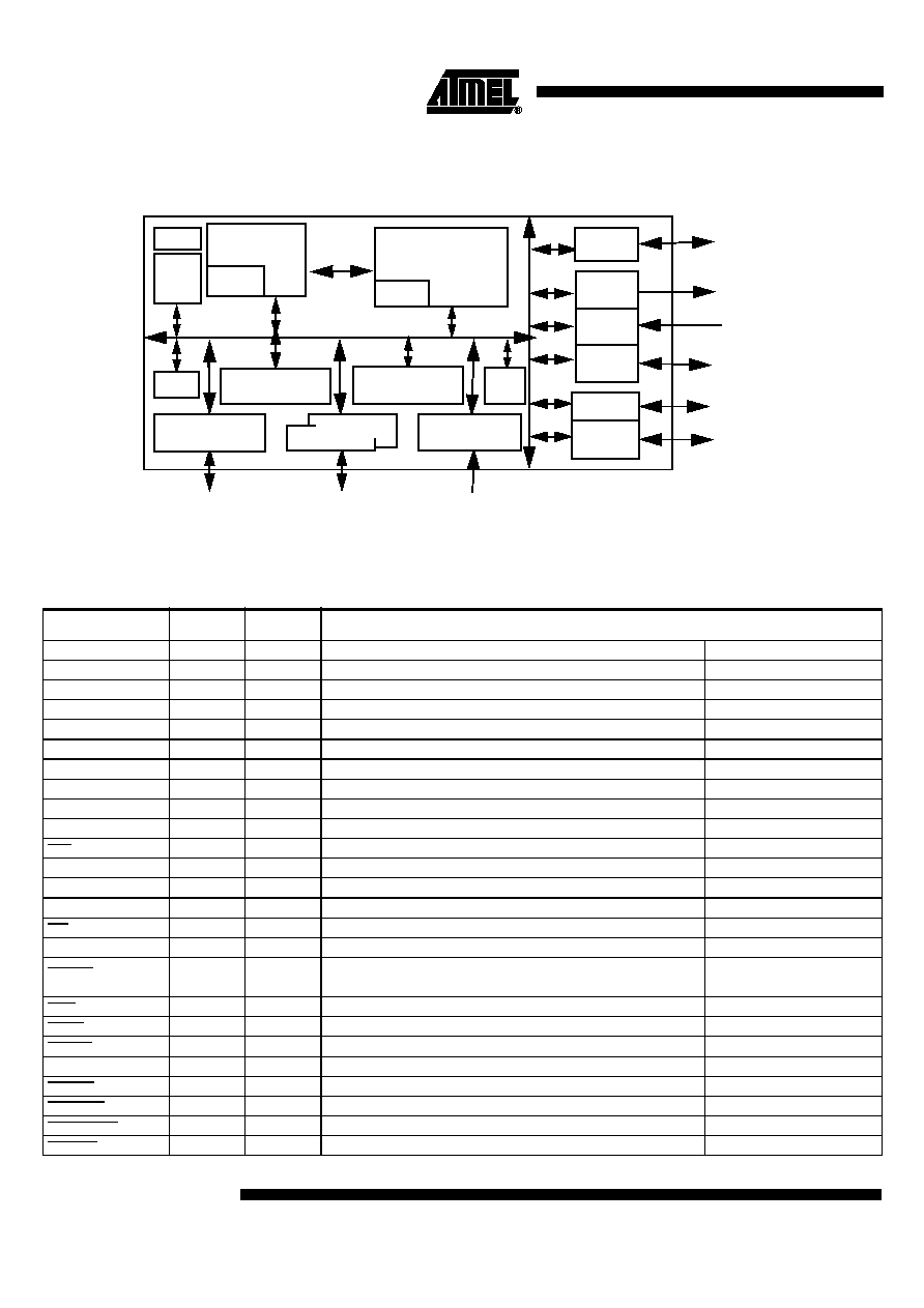
Block Diagram
Figure 1. TSC695F Block Diagram
Pin Descriptions
For pin assignment, refer to package section.
General Purpose
Interface
UART A
TAP
Clock
Managt
Error
Managt
General Purpose
Timer
Real Time Clock
Timer
32-bit
Integer
Unit
DMA
Arbiter
Access
Controller
Address
Interface
Wait State
Controller
Interrupts
RxD, TxD
GPI bits
DMA Ctrl
Mem Ctrl
Ready/Busy
Add.+Size+ASI
Data+Check bits
Parities
EDAC
Watch
Dog
Parity
Parity
Gen./Check.
Reset
&
UART B
Interrupt
Controller
32/64-bit
Floating-Point
Unit
Parity
Gen./Chk.
Gen./Chk.
Table 1. Pin Descriptions
Signal
Type
Active
Description
RA[31:0]
I/O,
32-bit registered address bus
Output buffer: 400 pF
RAPAR
I/O
High
Registered address bus parity
-
RASI[3:0]
I/O
4-bit registered address space identifier
-
RSIZE[1:0]
I/O
2-bit registered bus transaction size
-
RASPAR
I/O
High
Registered ASI and SIZE parity
-
CPAR
I/O
High
Control bus parity
-
D[31:0]
I/O
32-bit data bus
-
CB[6:0]
I/O
7-bit check-bit bus
-
DPAR
I/O
High
Data bus parity
-
RLDSTO
I/O
High
Registered atomic load-store
-
ALE
O
Low
Address latch enable
-
DXFER
I/O
High
Data transfer
-
LOCK
I/O
High
Bus lock
-
RD
I/O
High
Read access
-
WE
I/O
Low
Write enable
-
WRT
I/O
High
Advanced write
-
MHOLD
O
Low
Memory bus hold
MHOLD+FHOLD
+BHOLD+FCCV
MDS
O
Low
Memory data strobe
-
MEXC
O
Low
Memory exception
-
PROM8
I
Low
Select 8-bit wide PROM
-
BA[1:0]
O
Latched address used for 8-bit wide boot PROM
-
ROMCS
O
Low
PROM chip select
-
ROMWRT
I
Low
ROM write enable
-
MEMCS[9:0]
O
Low
Memory chip select
Output buffer: 400 pF
MEMWR
O
Low
Memory write strobe
Output buffer: 400 pF

3
TSC695F
4118H≠AERO≠06/03
Note:
If not specified, the output buffer type is 150 pF, the input buffer type is TTL.
OE
O
Low
Memory output enable
Output buffer: 400 pF
BUFFEN
O
Low
Data buffer enable
-
DDIR
O
High
Data buffer direction
-
DDIR
O
Low
Data buffer direction
-
IOSEL[3:0]
O
Low
I/O chip select
-
IOWR
O
Low
I/O and exchange memory write strobe
-
EXMCS
O
Low
Exchange memory chip select
-
BUSRDY
I
Low
Bus ready
-
BUSERR
I
Low
Bus error
-
DMAREQ
I
Low
DMA request
-
DMAGNT
O
Low
DMA grant
-
DMAAS
I
High
DMA address strobe
-
DRDY
O
Low
Data ready during DMA access
-
IUERR
O
Low
IU error
-
CPUHALT
O
Low
Processor (IU & FPU) halt and freeze
-
SYSERR
O
Low
System error
-
SYSHALT
I
Low
System halt
-
SYSAV
O
High
System availability
-
NOPAR
I
Low
No parity
-
INULL
O
High
Integer unit nullify cycle
-
INST
O
High
Instruction fetch
Used to check the execute
stage of IU
instruction pipeline
FLUSH
O
High
FPU instruction flush
DIA
O
High
Delay instruction annulled
RTC
O
High
Real Time Clock Counter output
-
RxA/RxB
I
Receive data UART 'A' and 'B'
Input trigger
TxA/TxB
O
Transmit data UART 'A' and 'B'
-
GPI[7:0]
I/O
GPI input/output
Input trigger
GPIINT
O
High
GPI interrupt
-
EXTINT[4:0]
I
External interrupt
Input trigger
EXTINTACK
O
High
External interrupt acknowledge
-
IWDE
I
High
Internal watch dog enable
-
EWDINT
I
High
External watch dog input interrupt
Input trigger
WDCLK
I
Watch dog clock
-
CLK2
I
Double frequency clock
-
SYSCLK
O
System clock
-
RESET
O
Low
Output reset
-
SYSRESET
I
Low
System input reset
Input trigger
TMODE[1:0]
I
Factory test mode
Functional mode=00
DEBUG
I
High
Software debug mode
-
TCK
I
Test (JTAG) clock
-
TRST
I
Low
Test (JTAG) reset
pull-up
37 k
TMS
I
Test (JTAG) mode select
pull-up
37 k
TDI
I
Test (JTAG) data input
pull-up
37 k
TDO
O
Test (JTAG) data output
-
VCCI/VSSI
Main internal power
-
VCCO/VSSO
Output driver power
-
Table 1. Pin Descriptions (Continued)
Signal
Type
Active
Description
4
TSC695F
4118H≠AERO≠06/03
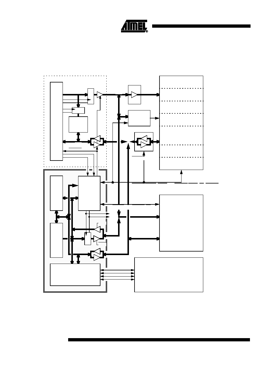
System Architecture
The TSC695F is to be used as an embedded processor requiring only memory and
application specific peripherals to be added to form a complete on-board computer. All
other system support functions are provided by the core.
Figure 2. System Architecture Based on TSC695F
IU
FPU
Memory
AL
E
SY
SCLK
A[31:0]
RA
[3
1:0
]
Ma
st
e
r
Ax[31:0]
TSC695F
DMA Unit
Local
Memory
DMAGNT
DMAREQ
DMAAS
RAMCtrl
(ROMCS, EXMCS, IOSEL[3:0], MEMWR, IOWR, OE, BUSRDY,...)
D[31
:0]
(0 WS)
RAM
CB
[6:0]
D
PA
R
Boot PROM
Xtd PROM
Xchg Mem
Xtd RAM
Xtd I/O
Xtd general
I/O 0
to
I/O 3
Memory
Glue
Logic
DMA
DMA
(MEMCS[9:0], MEMWR, OE)
(BUFFEN, DDIR)
Interface
User
Peripherals
Application
MEMCtrl

5
TSC695F
4118H≠AERO≠06/03
P
roduct
D
escription
Integer Unit
The Integer Unit (IU) is designed for highly dependable space and military applications,
and includes support for error detection. The RISC architecture makes the creation of a
processor that can execute instructions at a rate approaching one instruction per pro-
cessor clock possible.
To achieve that rate of execution, the IU employs a four-stage instruction pipeline that
permits parallel execution of multiple instructions.
∑
Fetch - The processor outputs the instruction address to fetch the instruction.
∑
Decode - The instruction is placed in the instruction register and is decoded. The
processor reads the operands from the register file and computes the next
instruction address.
∑
Execute - The processor executes the instruction and saves the results in temporary
registers. Pending traps are prioritized and internal traps are taken during this stage.
∑
Write - If no trap is taken, the processor writes the result to the destination register.
All four stages operate in parallel, working on up to four different instructions at a time. A
basic `single-cycle' instruction enters the pipeline and completes infour cycles.
By the time it reaches the write stage, three more instructions have entered and are
moving through the pipeline behind it. So, after the first four cycles, a single-cycle
instruction exits the pipeline and a single-cycle instruction enters the pipeline on every
cycle. Of course, a 'single-cycle' instruction actually takes four cycles to complete, but
they are called single cycle because with this type of instruction the processor can com-
plete one instruction per cycle after the initial four-cycle delay.
Floating-point Unit
The FLoating Point Unit (FPU) is designed to provide execution of single and double-
precision floating-point instructions concurrently with execution of integer instructions by
the IU. The FPU is compliant to the ANSI/IEEE-754 (1985) floating-point standard.
The FPU is designed for highly dependable space and military applications, and
includes support for concurrent error detection and testability.
The FPU uses a four stage instruction pipeline consisting of fetch, decode, execute and
write stages (F, D, E and W). The fetch unit captures instructions and their addresses
from the data and address buses. The decode unit contains logic to decode the floating-
point instruction opcodes. The execution unit handles all instruction execution. The exe-
cution unit includes a floating-point queue (FP queue), which contains stored floating-
point operate (FPop) instructions under execution and their addresses. The execution
unit controls the load unit, the store unit, and the datapath unit. The FPU depends upon
the IU to access all addresses and control signals for memory access. Floating-point
loads and stores are executed in conjunction with the IU, which provides addresses and
control signals while the FPU supplies or stores the data. Instruction fetch for integer
and floating-point instructions is provided by the IU.
The FPU provides three types of registers: f registers, FSR, and the FP queue. The FSR
is a 32-bit status and control register. It keeps track of rounding modes, floating-point
trap types, queue status, condition codes, and various IEEE exception information. The
floating-point queue contains the floating-point instruction currently under execution,
along with its corresponding address.