 | –≠–ª–µ–∫—Ç—Ä–æ–Ω–Ω—ã–π –∫–æ–º–ø–æ–Ω–µ–Ω—Ç: 80C32E | –°–∫–∞—á–∞—Ç—å:  PDF PDF  ZIP ZIP |

Rev. 4149M≠AERO≠06/04
1
Features
∑
8032 Pin and Instruction Compatible
∑
Four 8-bit I/O Ports
∑
Three 16-bit Timer/Counters
∑
256 bytes RAM
∑
Full-duplex UART
∑
Asynchronous Port Reset
∑
6 Sources, 2 Level Interrupt Structure
∑
64 Kbytes Program Memory Space
∑
64 Kbytes Data Memory Space
∑
Power Control Modes
∑
Idle Mode
∑
Power-down Mode
∑
On-chip Oscillator
∑
Operating Frequency: 30 MHz
∑
Power Supply: 4.5V to 5.5V
∑
Temperature Range: Military (-55
o
C to 125
o
C)
∑
No Single Event Latch-up below a LET Threshold of 80 MeV/mg/cm
2
∑
Tested up to a Total Dose of 30 krads (Si) according to MIL STD 883 Method 1019
∑
Packages: Side Brazed 40-pin, MQFPJ 44-pin
∑
QML Q and V with SMD 5962-00518
∑
SCC C an B with Specification SCC9521002
Description
The 80C32E is a radiation tolerant ROMless version of the 80C52 single chip 8-bit
microcontroller.
The 80C32E retains all the features of the 80C32 with 256 bytes of internal RAM, a 6-
source, 2-level interrupt system, an on-chip oscillator and three 16-bit timer/counters.
The fully static design of the 80C32E reduces system power consumption by bringing
the clock frequency down to any value, even DC, without loss of data.
The 80C32E has 2 software-selectable modes of reduced activity for further reduction
in power consumption. In the idle mode the CPU is frozen while the timers, the serial
port and the interrupt system are still operating. In the power-down mode the RAM is
saved and all other functions are inoperative.
Rad. Tolerant
8-bit ROMless
Microcontroller
80C32E

2
80C32E
4149M≠AERO≠06/04
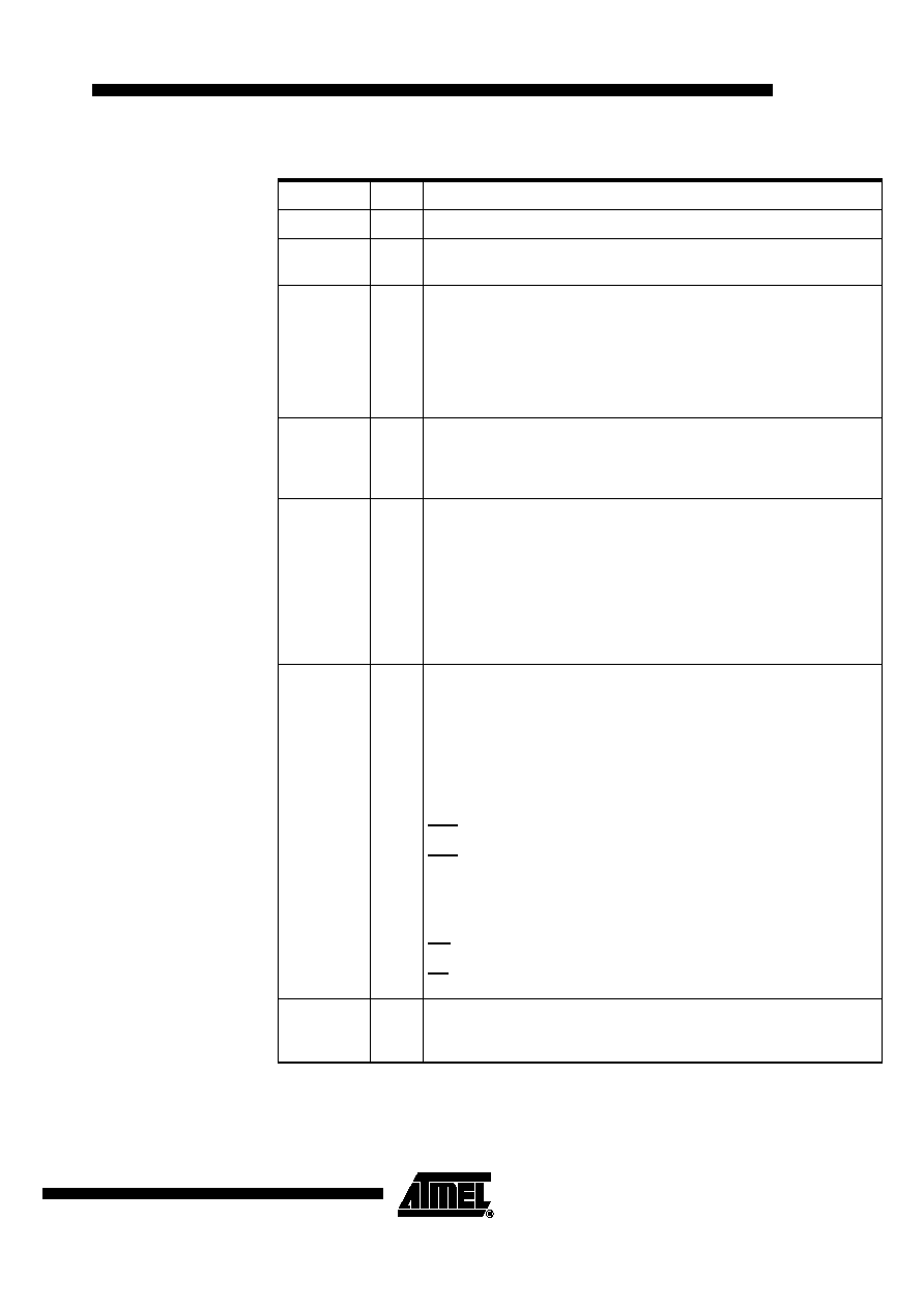
Block Diagram
Pin Configuration
Note:
NIC: No Internal Connection
Timer 0
INT
RAM
256x8
T0
T1
Rx
D
Tx
D
WR
RD
EA
PSEN
ALE
XTAL2
XTAL1
UART
CPU
INT
1
Ctrl
INT
0
C51
CORE
Port 0
P0
Port 1 Port 2 Port 3
Parallel I/O Ports & Ext. Bus
P1
P2
P3
IB-bus
RS
T
Timer 1
Timer 2
T2
T2
E
X
5 4 3 2 1
6
44 43 42 41 40
P1
.
4
P1
.
0
P1
.
1
P1
.
3
P1
.
2
NIC*
VC
C
P
0
.0
/A
D0
P
0
.2
/A
D2
P
0
.1
/A
D1
P0.4/AD4
P0.6/AD6
P0.5/AD5
P0.7/AD7
ALE
PSEN
EA
NIC*
P2.7/A15
P2.5/A13
P2.6/A14
P
3
.6/W
R
P
3
.7/RD
XT
AL
2
XT
AL
1
VS
S
P
2
.0/A
8
P
2
.1/A
9
P
2
.2/A
10
P
2
.3/A
1
1
P
2
.4/A
12
P1.5
P1.6
P1.7
RST
P3.0/RxD
NIC*
P3.1/TxD
P3.2/INT0
P3.3/INT1
P3.4/T0
P3.5/T1
P
0
.3/A
D3
NIC*
7
8
9
10
11
12
13
14
15
16
17
39
38
37
36
35
34
33
32
31
30
29
MQFPJ44
18 19 20 21 22 23 24 25 26 27 28
P1.7
RST
P3.0/RxD
P3.1/TxD
P1.3
1
P1.5
P3.2/INT0
P3.3/INT1
P3.5/T1
P3.6/WR
P3.7/RD
XTAL2
XTAL1
VSS
P2.0/A8
P2.1/A9
P2.2/A10
P2.3/A11
P2.4/A12
P0.4/A4
P0.6/A6
P0.5/A5
P0.7/A7
ALE
PSEN
EA/VPP
P2.7/A15
P2.5/A13
P2.6/A14
P1.0/T2
P1.1/T2EX
VCC
P0.0/A0
P0.1/A1
P0.2/A2
P0.3/A3
2
3
4
5
6
7
8
9
10
11
12
13
14
15
16
17
18
19
20
40
39
38
37
36
35
34
33
32
31
30
29
28
27
26
25
24
23
22
21
SB40
P1.6
P1.4
P1.2
P3.4/T0
3
80C32E
4149M≠AERO≠06/04
Pin Description
Mnemonic
Type
Name and Function
V
SS
I
Ground: 0V reference
V
CC
I
Power Supply: This is the power supply voltage for normal, idle and
power-down operation
P0.0-P0.7
I/O
Port 0: Port 0 is an open-drain, bidirectional I/O port. Port 0 pins that
have 1s written to them float and can be used as high impedance inputs.
Port 0 pins must be polarized to Vcc or Vss in order to prevent any
parasitic current consumption. Port 0 is also the multiplexed low-order
address and data bus during access to external program and data
memory. In this application, it uses strong internal pull-up when emitting
1s.
P1.0-P1.7
I/O
Port 1: Port 1 is an 8-bit bidirectional I/O port with internal pull-ups. Port 1
pins that have 1s written to them are pulled high by the internal pull-ups
and can be used as inputs. As inputs, Port 1 pins that are externally
pulled low will source current because of the internal pull-ups.
P2.0-P2.7
I/O
Port 2: Port 2 is an 8-bit bidirectional I/O port with internal pull-ups. Port 2
pins that have 1s written to them are pulled high by the internal pull-ups
and can be used as inputs. As inputs, Port 2 pins that are externally
pulled low will source current because of the internal pull-ups. Port 2
emits the high-order address byte during fetches from external program
memory and during accesses to external data memory that use 16-bit
addresses (MOVX @DPTR).In this application, it uses strong internal
pull-ups emitting 1s. During accesses to external data memory that use
8-bit addresses (MOVX @Ri), port 2 emits the contents of the P2 SFR.
P3.0-P3.7
I/O
Port 3: Port 3 is an 8-bit bidirectional I/O port with internal pull-ups. Port 3
pins that have 1s written to them are pulled high by the internal pull-ups
and can be used as inputs. As inputs, Port 3 pins that are externally
pulled low will source current because of the internal pull-ups. Port 3 also
serves the special features of the 80C51 family, as listed below.
I
RXD (P3.0): Serial input port
O
TXD (P3.1): Serial output port
I
INT0 (P3.2): External interrupt 0
I
INT1 (P3.3): External interrupt 1
I
T0 (P3.4): Timer 0 external input
I
T1 (P3.5): Timer 1 external input
O
WR (P3.6): External data memory write strobe
O
RD (P3.7): External data memory read strobe
RST
I
Reset: A high on this pin for two machine cycles while the oscillator is
running, resets the device. An internal diffused resistor to V
SS
permits a
power-on reset using only an external capacitor to V
CC.
4
80C32E
4149M≠AERO≠06/04
ALE
O (I)
Address Latch Enable: Output pulse for latching the low byte of the
address during an access to external memory. In normal operation, ALE
is emitted at a constant rate of 1/6 the oscillator frequency, and can be
used for external timing or clocking. Note that one ALE pulse is skipped
during each access to external data memory.
PSEN
O
Program Store ENable: The read strobe to external program memory.
When executing code from the external program memory, PSEN is
activated twice each machine cycle, except that two PSEN activations
are skipped during each access to external data memory. PSEN is not
activated during fetches from internal program memory.
EA
I
External Access Enable: EA must be externally held low to enable the
device to fetch code from external program memory locations.
XTAL1
I
Crystal 1: Input to the inverting oscillator amplifier and input to the
internal clock generator circuits.
XTAL2
O
Crystal 2: Output from the inverting oscillator amplifier
Mnemonic
Type
Name and Function

5
80C32E
4149M≠AERO≠06/04
Idle and Power-down
Operation
Idle mode allows the interrupt, serial port and timer blocks to continue to operate while
the clock of the CPU is gated off.
Power-down mode stops the oscillator.
Table 1. PCON Register
PCON ≠ Power Control Register
Reset Value = 000X 0000
Not bit addressable
7
6
5
4
3
2
1
0
SMOD
-
-
-
GF1
GF0
PD
IDL
Bit
Number
Bit
Mnemonic
Description
7
SMOD
Double Baud Rate bit
Set to select double baud rate in mode 1, 2 or 3.
6
-
Reserved
The value read from this bit is indeterminate. Do not set this bit.
5
-
Reserved
The value read from this bit is indeterminate. Do not set this bit.
4
-
Reserved
The value read from this bit is indeterminate. Do not set this bit.
3
GF1
General-purpose Flag
Cleared by user for General-purpose usage.
Set by user for General-purpose usage.
2
GF0
General-purpose Flag
Cleared by user for General-purpose usage.
Set by user for General-purpose usage.
1
PD
Power-down mode bit
Cleared by hardware when reset occurs.
Set to enter power-down mode.
0
IDL
Idle mode bit
Clear by hardware when interrupt or reset occurs.
Set to enter idle mode.