1
Features
∑
Single-voltage Operation
≠ 5V Read
≠ 5V Programming
∑
Fast Read Access Time ≠ 70 ns
∑
Internal Erase/Program Control
∑
Sector Architecture
≠ One 8K Word (16K Bytes) Boot Block with Programming Lockout
≠ Two 4K Word (8K Bytes) Parameter Blocks
≠ One 496K Word (992K Bytes) Main Memory Array Block
∑
Fast Sector Erase Time ≠ 10 seconds
∑
Byte-by-byte or Word-by-word Programming ≠ 10 µs Typical
∑
Hardware Data Protection
∑
Data Polling for End of Program Detection
∑
Low Power Dissipation
≠ 50 mA Active Current
≠ 100 µA CMOS Standby Current
∑
Typical 10,000 Write Cycles
Description
The AT49F008A(T) and AT49F8192A(T) are 5-volt, 8-megabit Flash memories orga-
nized as 1,048,576 words of 8 bits each or 512K words of 16 bits each. Manufactured
with Atmel's advanced nonvolatile CMOS technology, the devices offer access times
to 90 ns with power dissipation of just 275 mW. When deselected, the CMOS standby
current is less than 100 µA.
The device contains a user-enabled "boot block" protection feature. Two versions of
the feature are available: the AT49F008A/8192A locates the boot block at lowest
order addresses ("bottom boot"); the AT49F008AT/8192AT locates it at highest order
addresses ("top boot").
To allow for simple in-system reprogrammability, the AT49F008A(T)/8192A(T) does
not require high-input voltages for programming. Reading data out of the device is
similar to reading from an EPROM; it has standard CE, OE and WE inputs to avoid
bus contention. Reprogramming the AT49F008A(T)/8192A(T) is performed by first
erasing a block of data and then programming on a byte-by-byte or word-by-word
basis.
8-megabit
(1M x 8/
512K x 16)
Flash Memory
AT49F008A
AT49F008AT
AT49F8192A
AT49F8192AT
Rev. 1199G≠FLASH≠11/02
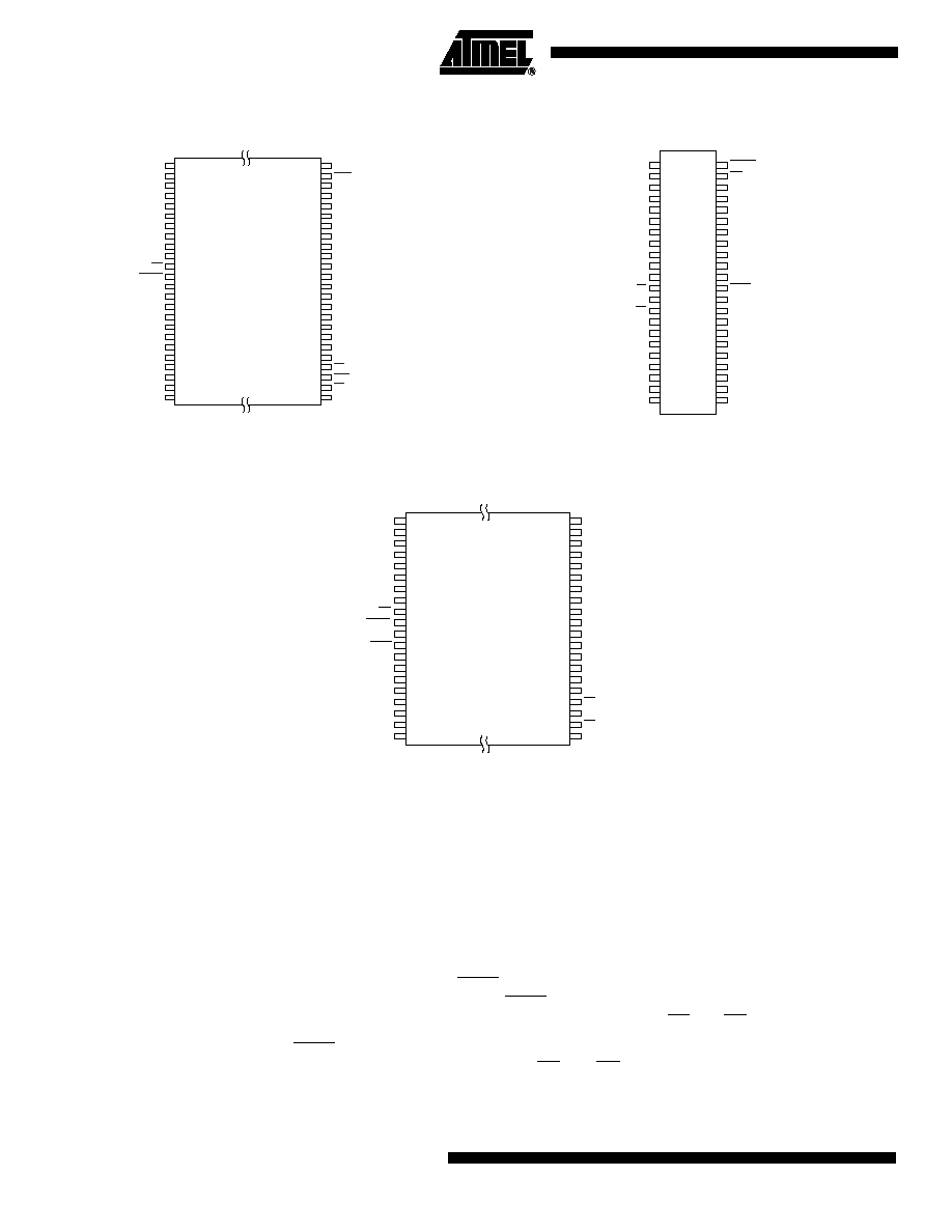
Pin Configurations
Pin Name
Function
A0 - A18
Addresses
CE
Chip Enable
OE
Output Enable
WE
Write Enable
RESET
Reset
RDY/BUSY
Ready/Busy Output
I/O0 - I/O14
Data Inputs/Outputs
I/O15 (A-1)
I/O15 (Data Input/Output, Word Mode)
A-1 (LSB Address Input, Byte Mode)
BYTE
Selects Byte or Word Mode
NC
No Connect
2
AT49F008A(T)/8192A(T)
1199G≠FLASH≠11/02
AT49F8192A(T) TSOP Top View
Type 1
1
2
3
4
5
6
7
8
9
10
11
12
13
14
15
16
17
18
19
20
21
22
23
24
48
47
46
45
44
43
42
41
40
39
38
37
36
35
34
33
32
31
30
29
28
27
26
25
A15
A14
A13
A12
A11
A10
A9
A8
NC
NC
WE
RESET
NC
NC
NC
A18
A17
A7
A6
A5
A4
A3
A2
A1
A16
BYTE
GND
I/O15 / A-1
I/O7
I/O14
I/O6
I/O13
I/O5
I/O12
I/O4
VCC
I/O11
I/O3
I/O10
I/O2
I/O9
I/O1
I/O8
I/O0
OE
GND
CE
A0
AT49F008A(T) TSOP Top View
Type 1
1
2
3
4
5
6
7
8
9
10
11
12
13
14
15
16
17
18
19
20
40
39
38
37
36
35
34
33
32
31
30
29
28
27
26
25
24
23
22
21
A16
A15
A14
A13
A12
A11
A9
A8
WE
RESET
NC
RDY/BUSY
A18
A7
A6
A5
A4
A3
A2
A1
A17
GND
NC
A-1
A10
I/O7
I/O6
I/O5
I/O4
VCC
VCC
NC
I/O3
I/O2
I/O1
I/O0
OE
GND
CE
A0
AT49F8192A(T) SOIC (SOP) Top View
1
2
3
4
5
6
7
8
9
10
11
12
13
14
15
16
17
18
19
20
21
22
44
43
42
41
40
39
38
37
36
35
34
33
32
31
30
29
28
27
26
25
24
23
NC
A18
A17
A7
A6
A5
A4
A3
A2
A1
A0
CE
GND
OE
I/O0
I/O8
I/O1
I/O9
I/O2
I/O10
I/O3
I/O11
RESET
WE
A8
A9
A10
A11
A12
A13
A14
A15
A16
BYTE
GND
I/O15
I/O7
I/O14
I/O6
I/O13
I/O5
I/O12
I/O4
VCC
Note:
"∑" denotes a white dot marked on the package.
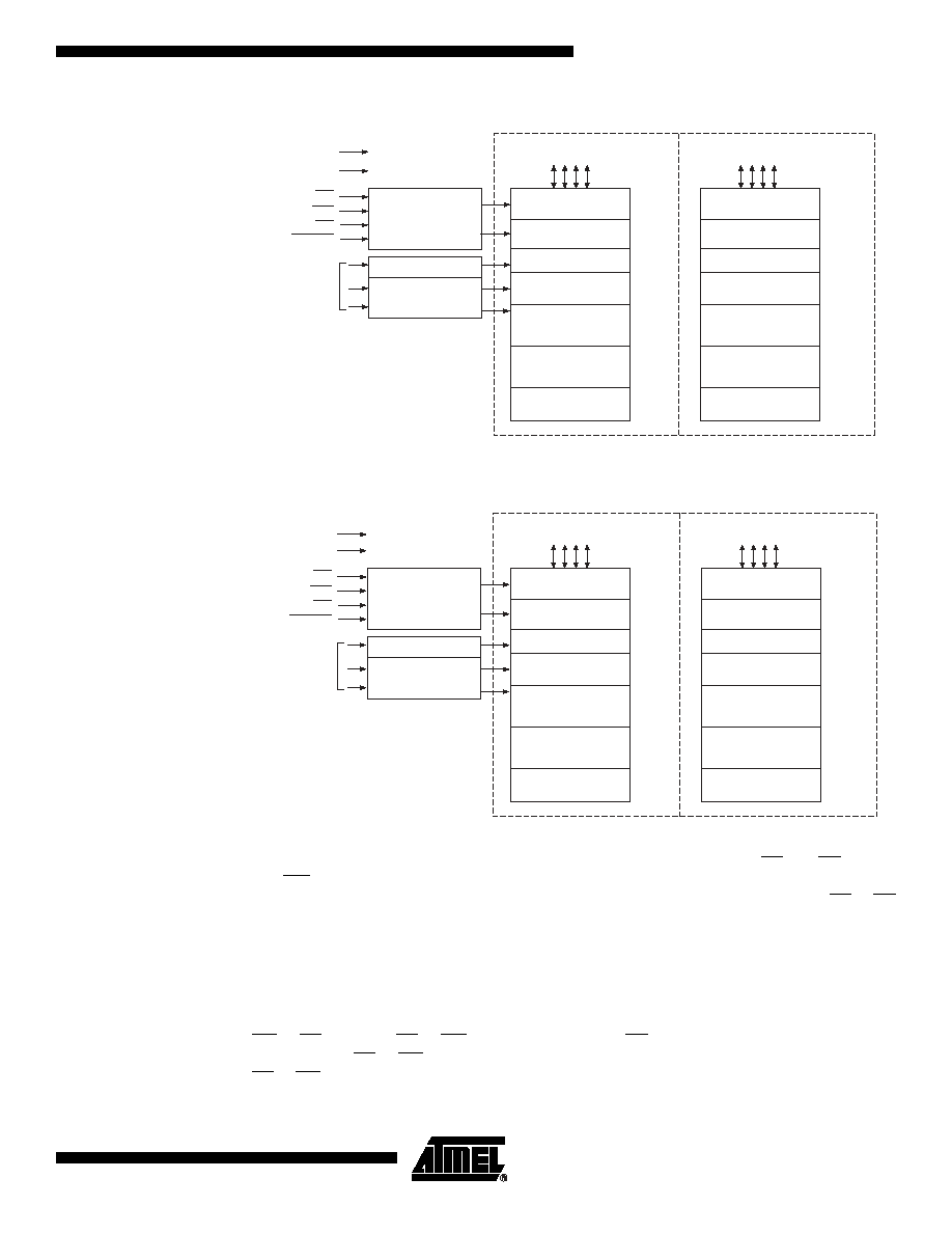
The device is erased by executing the Erase command sequence; the device internally con-
trols the erase operation. The memory is divided into four blocks for erase operations. There
are two 4K word parameter block sections: the boot block, and the main memory array block.
The typical number of program and erase cycles is in excess of 10,000 cycles.
The optional 8K word boot block section includes a reprogramming lockout feature to provide
data integrity. This feature is enabled by a command sequence. Once the boot block program-
ming lockout feature is enabled, the data in the boot block cannot be changed when input
levels of 5.5 volts or less are used. The boot sector is designed to contain user secure code.
For the AT49F8192A(T), the BYTE pin controls whether the device data I/O pins operate in
the byte or word configuration. If the BYTE pin is set at a logic "1" or left open, the device is in
word configuration, I/O0 - I/O15 are active and controlled by CE and OE.
If the BYTE pin is set at logic "0", the device is in byte configuration, and only data I/O pins
I/O0 - I/O7 are active and controlled by CE and OE. The data I/O pins I/O8 - I/O14 are tri-
stated and the I/O15 pin is used as an input for the LSB (A-1) address function.
3
AT49F008A(T)/8192A(T)
1199G≠FLASH≠11/02
AT49F008A(T)
Block Diagram
AT49F8192A(T)
Block Diagram
Device
Operation
READ: The AT49F008A(T)/8192A(T) is accessed like an EPROM. When CE and OE are low
and WE is high, the data stored at the memory location determined by the address pins is
asserted on the outputs. The outputs are put in the high-impedance state whenever CE or OE
is high. This dual line control gives designers flexibility in preventing bus contention.
COMMAND SEQUENCES: When the device is first powered on, it will be reset to the read or
standby mode, depending upon the state of the control line inputs. In order to perform other
device functions, a series of command sequences are entered into the device. The command
sequences are shown in the Command Definitions table (I/O8 - I/O15 are don't care inputs for
the command codes). The command sequences are written by applying a low pulse on the
WE or CE input with CE or WE low (respectively) and OE high. The address is latched on the
falling edge of CE or WE, whichever occurs last. The data is latched by the first rising edge of
CE or WE. Standard microprocessor write timings are used. The address locations used in the
command sequences are not affected by entering the command sequences.
VCC
GND
OE
CONTROL
LOGIC
DATA INPUTS/OUTPUTS
I/O0 - I/O7
DATA INPUTS/OUTPUTS
I/O0 - I/O7
WE
CE
RESET
ADDRESS
INPUTS
Y DECODER
INPUT/OUTPUT
BUFFERS
INPUT/OUTPUT
BUFFERS
PROGRAM DATA
LATCHES
PROGRAM DATA
LATCHES
Y-GATING
AT49F008A
AT49F008AT
Y-GATING
FFFFF
FFFFF
MAIN MEMORY
(992K BYTES)
BOOT BLOCK
16K BYTES
PARAMETER
BLOCK 2
8K BYTES
PARAMETER
BLOCK 1
8K BYTES
PARAMETER
BLOCK 1
8K BYTES
PARAMETER
BLOCK 2
8K BYTES
BOOT BLOCK
16K BYTES
MAIN MEMORY
(992K BYTES)
08000
07FFF
FC000
FBFFF
06000
05FFF
FA000
F9FFF
X DECODER
04000
03FFF
F8000
F7FFF
00000
00000
VCC
GND
OE
CONTROL
LOGIC
DATA INPUTS/OUTPUTS
I/O0 - I/O15
DATA INPUTS/OUTPUTS
I/O0 - I/O15
WE
CE
RESET
ADDRESS
INPUTS
Y DECODER
INPUT/OUTPUT
BUFFERS
INPUT/OUTPUT
BUFFERS
PROGRAM DATA
LATCHES
PROGRAM DATA
LATCHES
Y-GATING
AT49F8192A
AT49F8192AT
Y-GATING
7FFFF
7FFFF
MAIN MEMORY
(496K WORDS)
BOOT BLOCK
8K WORDS
PARAMETER
BLOCK 2
4K WORDS
PARAMETER
BLOCK 1
4K WORDS
PARAMETER
BLOCK 1
4K WORDS
PARAMETER
BLOCK 2
4K WORDS
BOOT BLOCK
8K WORDS
MAIN MEMORY
(496K WORDS)
04000
03FFF
7E000
7DFFF
03000
02FFF
7D000
7CFFF
X DECODER
02000
01FFF
7C000
7BFFF
00000
00000

4
AT49F008A(T)/8192A(T)
1199G≠FLASH≠11/02
RESET: A RESET input pin is provided to ease some system applications. When RESET is at
a logic high level, the device is in its standard operating mode. A low level on the RESET input
halts the present device operation and puts the outputs of the device in a high-impedance
state. When a high level is reasserted on the RESET pin, the device returns to the read or
standby mode, depending upon the state of the control inputs. By applying a 12V ± 0.5V input
signal to the RESET pin, the boot block array can be reprogrammed even if the boot block pro-
gram lockout feature has been enabled (see Boot Block Programming Lockout Override
section).
ERASURE: Before a byte or word can be reprogrammed, it must be erased. The erased state
of memory bits is a logic "1". The entire device can be erased by using the Chip Erase com-
mand or individual sectors can be erased by using the Sector Erase command.
CHIP ERASE: The entire device can be erased at one time by using the 6-byte chip erase
software code. After the chip erase has been initiated, the device will internally time the erase
operation so that no external clocks are required. The maximum time to erase the chip is t
EC
.
If the boot block lockout has been enabled, the chip erase will not erase the data in the boot
block; it will erase the main memory block and the parameter blocks only. After the chip erase,
the device will return to the read or standby mode.
SECTOR ERASE: As an alternative to a full chip erase, the device is organized into four sec-
tors that can be individually erased. There are two 4K word parameter block sections, one
boot block, and the main memory array block. The Sector Erase command is a six-bus cycle
operation. The sector address is latched on the falling WE edge of the sixth cycle while the
30H data input command is latched at the rising edge of WE. The sector erase starts after the
rising edge of WE of the sixth cycle. The erase operation is internally controlled; it will auto-
matically time to completion. Whenever the main memory block is erased and reprogrammed,
the two parameter blocks should be erased and reprogrammed before the main memory block
is erased again. Whenever a parameter block is erased and reprogrammed, the other param-
eter block should be erased and reprogrammed before the first parameter block is erased
again. Whenever the boot block is erased and reprogrammed, the main memory block and the
parameter blocks should be erased and reprogrammed before the boot block is erased again.
BYTE/WORD PROGRAMMING: Once a memory block is erased, it is programmed (to a logic
"0") on a byte-by-byte or word-by-word basis. Programming is accomplished via the internal
device command register and is a four-bus cycle operation. The device will automatically gen-
erate the required internal program pulses.
Any commands written to the chip during the embedded programming cycle will be ignored. If
a hardware reset happens during programming, the data at the location being programmed
will be corrupted. Please note that a data "0" cannot be programmed back to a "1"; only erase
operations can convert "0"s to "1"s. Programming is completed after the specified t
BP
cycle
time. The Data Polling feature may also be used to indicate the end of a program cycle.
BOOT BLOCK PROGRAMMING LOCKOUT: The device has one designated block that has
a programming lockout feature. This feature prevents programming of data in the designated
block once the feature has been enabled. The size of the block is 8K words. This block,
referred to as the boot block, can contain secure code that is used to bring up the system.
Enabling the lockout feature will allow the boot code to stay in the device while data in the rest
of the device is updated. This feature does not have to be activated; the boot block's usage as
a write-protected region is optional to the user. The address range of the boot block is 00000H
to 03FFFH for the AT49F008A; FC000H to FFFFFH for the AT49F008AT; 00000H to 01FFFH
for the AT49F8192A; and 7E000H to 7FFFFH for the AT49F8192AT.

5
AT49F008A(T)/8192A(T)
1199G≠FLASH≠11/02
Once the feature is enabled, the data in the boot block can no longer be erased or pro-
grammed when input levels of 5.5V or less are used. Data in the main memory block can still
be changed through the regular programming method. To activate the lockout feature, a series
of six program commands to specific addresses with specific data must be performed. Please
refer to the Command Definitions table.
BOOT BLOCK LOCKOUT DETECTION: A software method is available to determine if pro-
gramming of the boot block section is locked out. When the device is in the software product
identification mode (see Software Product Identification Entry and Exit sections), a read from
the following address location will show if programming the boot block is locked out ≠ 00002H
for the AT49F008A and AT49F8192A; FC002H for the AT49F008AT; and 7E002H for the
AT49F8192AT. If the data on I/O0 is low, the boot block can be programmed; if the data on
I/O0 is high, the program lockout feature has been enabled and the block cannot be pro-
grammed. The software product identification exit code should be used to return to standard
operation.
BOOT BLOCK PROGRAMMING LOCKOUT OVERRIDE: The user can override the boot
block programming lockout by taking the RESET pin to 12 volts during the entire chip erase,
sector erase or word programming operation. When the RESET pin is brought back to TTL
levels, the boot block programming lockout feature is again active.
PRODUCT IDENTIFICATION: The product identification mode identifies the device and man-
ufacturer as Atmel. It may be accessed by hardware or software operation. The hardware
operation mode can be used by an external programmer to identify the correct programming
algorithm for the Atmel product.
For details, see "Operating Modes" (for hardware operation) or "Software Product Identifica-
tion Entry/Exit" on page 13. The manufacturer and device codes are the same for both modes.
DATA POLLING: The AT49F008A(T)/8192A(T) features Data Polling to indicate the end of a
program cycle. During a program cycle an attempted read of the last byte loaded will result in
the complement of the loaded data on I/O7. Once the program cycle has been completed, true
data is valid on all outputs and the next cycle may begin. During a chip or sector erase opera-
tion, an attempt to read the device will give a "0" on I/O7. Once the program or erase cycle has
completed, true data will be read from the device. Data Polling may begin at any time during
the program cycle.
TOGGLE BIT: In addition to Data Polling, the AT49F008A(T)/8192A(T) provides another
method for determining the end of a program or erase cycle. During a program or erase oper-
ation, successive attempts to read data from the device will result in I/O6 toggling between
one and zero. Once the program cycle has completed, I/O6 will stop toggling and valid data
will be read. Examining the toggle bit may begin at any time during a program cycle.
READY/BUSY: For the AT49F008A(T), pin 12 is an open-drain Ready/Busy output pin, which
provides another method of detecting the end of a program or erase operation. RDY/BUSY is
actively pulled low during the internal program and erase cycles and it is released at the com-
pletion of the cycle. The open-drain connection allows for OR-tying of several devices to the
same RDY/BUSY line.
HARDWARE DATA PROTECTION: Hardware features protect against inadvertent programs
to the AT49F008A(T)/8192A(T) in the following ways: (a) V
CC
sense: if V
CC
is below 3.8V (typ-
ical), the program function is inhibited. (b) V
CC
power-on delay: once V
CC
has reached the V
CC
sense level, the device will automatically time-out 10 ms (typical) before programming. (c) Pro-
gram inhibit: holding any one of OE low, CE high or WE high inhibits program cycles. (d) Noise
filter: pulses of less than 15 ns (typical) on the WE or CE inputs will not initiate a program
cycle.