Rev. 4113A≠8051≠09/02
Features
∑
80C52 Compatible
≠ Four 8-bit I/O Ports
≠ Three 16-bit Timer/Counters
≠ 256 Bytes Scratch Pad RAM
≠ 8 Interrupt Sources with 4 Priority Levels
≠ Dual Data Pointer
∑
Variable Length MOVX for Slow RAM/Peripherals
∑
High-speed Architecture
≠ 10 to 40 MHz in Standard Mode
∑
16K/32K Bytes On-Chip ROM Program
∑
T80C51RD2 ROMless Versions
∑
On-Chip 1024 bytes Expanded RAM (XRAM)
≠ Software Selectable Size (0, 256, 512, 768, 1024 bytes)
≠ 256 Bytes Selected at Reset for AT87C51RB2/RC2 Compatibility
∑
Keyboard Interrupt Interface on Port P1
∑
8-bit Clock Prescaler
∑
64K Program and Data Memory Spaces
∑
Improved X2 Mode with Independant Selection for CPU and Each Peripheral
∑
Programmable Counter Array 5 Channels with:
≠
High-speed Output
≠
Compare/Capture
≠
Pulse Width Modulator
≠
Watchdog Timer Capabilities
∑
Asynchronous Port Reset
∑
Full Duplex Enhanced UART
∑
Dedicated Baud Rate Generator for UART
∑
Low EMI (Inhibit ALE)
∑
Hardware Watchdog Timer (One-time Enabled with Reset-out)
∑
Power Control Modes
≠ Idle Mode
≠ Power-down Mode
≠ Power-off Flag
∑
Power Supply: 2.7V to 5.5V or 2.7V to 3.6V
∑
Temperature Ranges: Commercial (0 to +70
∞
C) and Industrial (-40
∞
C to +85
∞
C)
∑
Packages: PDIL40, PLCC44, VQFP44
Description
AT8xC51Rx2 microcontrollers are high performance ROM versions of the 80C51 8-bit
microcontrollers. They contain a 0K, 16K or 32K bytes ROM memory block for
program.
The microcontrollers retain all features of the Atmel 80C52 with 256 bytes of internal
RAM, a 7-source 4-level interrupt controller and three timer/counters.
In addition, the microcontrollers have a Programmable Counter Array, an XRAM of
1024 byte, a Hardware Watchdog Timer, a Keyboard Interface, a more versatile serial
channel that facilitates multiprocessor communication (EUART) and a speed improve-
ment mechanism (X2 mode).
The microcontrollers have 2 software-selectable modes of reduced activity and 8 bit
clock prescaler for further reduction in power consumption. In Idle mode, the CPU is
frozen while the peripherals and the interrupt system are still operating. In the Power-
down mode, the RAM is saved and all other functions are inoperative.
80C51 High
Performance
ROM 8-bit
Microcontroller
AT80C51RD2
AT83C51RB2
AT83C51RC2
2
AT80C51RD2/AT83C51Rx2
4113A≠8051≠09/02
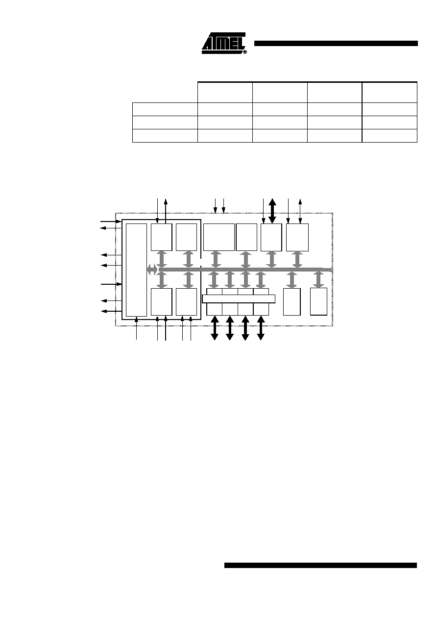
Table 1. Memory Size
Block Diagram
Notes:
1. Alternate function of Port 1
2. Alternate function of Port 3
ROM (Bytes)
XRAM (Bytes)
TOTAL RAM
(Bytes)
I/O
AT83C51RB2
16K
1024
1280
32
AT83C51RC2
32K
1024
1280
32
AT80C51RD2
ROMless
1024
1280
32
Timer 0
INT
RAM
256x8
T0
T1
Rx
D
Tx
D
WR
RD
EA
PSEN
ALE/
XTAL2
XTAL1
EUART
CPU
Timer 1
INT
1
Ctrl
INT
0
(2)
(2)
C51
CORE
(2) (2)
(2) (2)
Port 0
P0
Port 1 Port 2 Port 3
Parallel I/O Ports & Ext. Bus
P1
P2
P3
XRAM
1Kx8
IB-bus
PCA
R
ESE
T
PROG
Watch
Dog
PC
A
EC
I
Vs
s
VC
C
(2)
(2)
(1)
(1)
Timer2
T2
E
X
T2
(1)
(1)
ROM
32Kx8 or
16Kx8
Key
Board
+
BRG
3
AT80C51RD2/AT83C51Rx2
4113A≠8051≠09/02
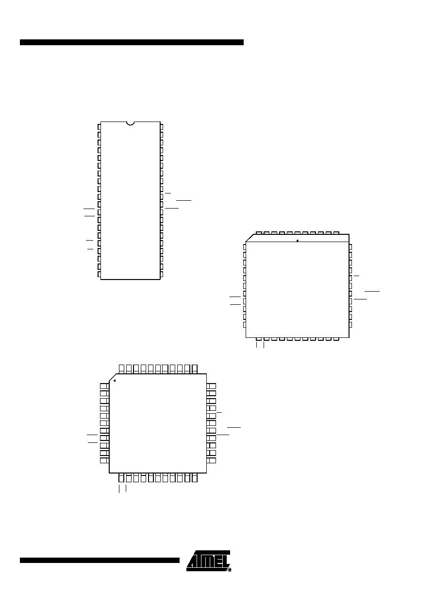
Pin Configurations
P1.7CEX4
P1.4/CEX1
RST
P3.0/RxD
P3.1/TxD
P1.3CEX0
1
P1.5/CEX2
P1.6/CEX3
P3.2/INT0
P3.3/INT1
P3.4/T0
P3.5/T1
P3.6/WR
P3.7/RD
XTAL2
XTAL1
VSS
P2.0/AD8
P2.1/AD9
P2.2/AD10
P2.3/AD11
P2.4/AD12
P0.4/AD4
P0.6/AD6
P0.5/AD5
P0.7/AD7
ALE/PROG
PSEN
EA
P2.7/AD15
P2.5/AD13
P2.6/AD14
P1.0/T2
P1.2/ECI
P1.1/T2EX
VCC
P0.0/AD0
P0.1/AD1
P0.2/AD2
P0.3/AD3
PDIL40
2
3
4
5
6
7
8
9
10
11
12
13
14
15
16
17
18
19
20
40
39
38
37
36
35
34
33
32
31
30
29
28
27
26
25
24
23
22
21
43 42 41 40 39
44
38 37 36 35 34
P1
.
4
/
C
E
X
1
P1
.
0
/
T
2
P1
.
1
/
T
2
E
X
P1
.
3
/
C
E
X
0
P1
.
2
/
E
C
I
NI
C*
VC
C
P0
.
0
/
A
D
0
P0
.
2
/
A
D
2
P0
.
3
/
A
D
3
P0
.
1
/
A
D
1
P0.4/AD4
P0.6/AD6
P0.5/AD5
P0.7/AD7
ALE/PROG
PSEN
EA
NIC*
P2.7/A15
P2.5/A13
P2.6/A14
P1.5/CEX2
P1.6/CEX3
P1.7/CEX4
RST
P3.0/RxD
NIC*
P3.1/TxD
P3.2/INT0
P3.3/INT1
P3.4/T0
P3.5/T1
P
3
.6
/W
R
P3
.
7
/
R
D
XT
A
L
2
XT
A
L
1
VS
S
P
2
.0
/A
8
P2
.
1
/
A
9
P
2
.2
/A
1
0
P
2
.3
/A
1
1
P
2
.4
/A
1
2
NI
C*
12 13
17
16
15
14
20
19
18
21 22
33
32
31
30
29
28
27
26
25
24
23
VQFP44 1.4
1
2
3
4
5
6
7
8
9
10
11
18 19
23
22
21
20
26
25
24
27 28
5
4
3
2
1
6
44 43 42 41 40
P
1
.4/CE
X
1
P
1
.0/T
2
P
1
.1/T
2E
X
P
1
.3/CE
X
0
P
1
.2/E
CI
NIC*
VC
C
P
0
.0/A
D0
P
0
.2/A
D2
P
0
.1/A
D1
P0.4/AD4
P0.6/AD6
P0.5/AD5
P0.7/AD7
ALE/PROG
PSEN
EA
NIC*
P2.7/A15
P2.5/A13
P2.6/A14
P3
.
6
/
W
R
P
3
.7
/RD
XT
AL
2
XT
AL
1
VSS
P
2
.0
/A
8
P
2
.1
/A
9
P
2
.2/A
1
0
P
2
.3/A
1
1
P
2
.4/A
1
2
P1.5/CEX2
P1.6/CEX3
P1.7/CEx4
RST
P3.0/RxD
NIC*
P3.1/TxD
P3.2/INT0
P3.3/INT1
P3.4/T0
P3.5/T1
P
0
.3/A
D3
NIC*
7
8
9
10
11
12
13
14
15
16
17
39
38
37
36
35
34
33
32
31
30
29
PLCC44
*NIC: No Internal Connection
4
AT80C51RD2/AT83C51Rx2
4113A≠8051≠09/02
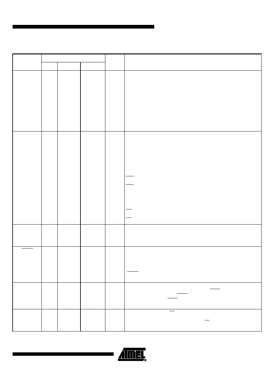
Table 2. Pin Description
Mnemonic
Pin Number
Type
Name and Function
DIL
PLCC44
VQFP44 1.4
V
SS
20
22
16
I
Ground: 0V reference
V
CC
40
44
38
I
Power Supply: This is the power supply voltage for normal, idle and power-down
operation
P0.0 - P0.7
39 - 32
43 - 36
37 - 30
I/O
Port 0: Port 0 is an open-drain, bi-directional I/O port. Port 0 pins that have 1s
written to them float and can be used as high impedance inputs. Port 0 must be
polarized to V
CC
or V
SS
in order to prevent any parasitic current consumption. Port
0 is also the multiplexed low-order address and data bus during access to external
program and data memory. In this application, it uses strong internal pull-up when
emitting 1s. Port 0 also inputs the code bytes during EPROM programming.
External pull-ups are required during program verification during which P0 outputs
the code bytes.
P1.0 - P1.7
1 - 8
2 - 9
40 - 44
1 - 3
I/O
Port 1: Port 1 is an 8-bit bi-directional I/O port with internal pull-ups. Port 1 pins
that have 1s written to them are pulled high by the internal pull-ups and can be
used as inputs. As inputs, Port 1 pins that are externally pulled low will source
current because of the internal pull-ups. Port 1 also receives the low-order address
byte during memory programming and verification.
Alternate functions for T89C51RB2/RC2 Port 1 include:
1
2
40
I/O
P1.0: Input/Output
I/O
T2 (P1.0): Timer/Counter 2 external count input/Clockout
2
3
41
I/O
P1.1: Input/Output
I
T2EX: Timer/Counter 2 Reload/Capture/Direction Control
3
4
42
I/O
P1.2: Input/Output
I
ECI: External Clock for the PCA
4
5
43
I/O
P1.3: Input/Output
I/O
CEX0: Capture/Compare External I/O for PCA module 0
5
6
44
I/O
P1.4: Input/Output
I/O
CEX1: Capture/Compare External I/O for PCA module 1
6
7
1
I/O
P1.5: Input/Output
I/O
CEX2: Capture/Compare External I/O for PCA module 2
7
8
2
I/O
P1.6: Input/Output
I/O
CEX3: Capture/Compare External I/O for PCA module 3
8
9
3
I/O
P1.7: Input/Output:
I/O
CEX4: Capture/Compare External I/O for PCA module 4
XTAL1
19
21
15
I
Crystal 1: Input to the inverting oscillator amplifier and input to the internal clock
generator circuits.
XTAL2
18
20
14
O
Crystal 2: Output from the inverting oscillator amplifier
5
AT80C51RD2/AT83C51Rx2
4113A≠8051≠09/02
P2.0 - P2.7
21 - 28
24 - 31
18 - 25
I/O
Port 2: Port 2 is an 8-bit bi-directional I/O port with internal pull-ups. Port 2 pins
that have 1s written to them are pulled high by the internal pull-ups and can be
used as inputs. As inputs, Port 2 pins that are externally pulled low will source
current because of the internal pull-ups. Port 2 emits the high-order address byte
during fetches from external program memory and during accesses to external
data memory that use 16-bit addresses (MOVX @DPTR). In this application, it
uses strong internal pull-ups emitting 1s. During accesses to external data memory
that use 8-bit addresses (MOVX @Ri), Port 2 emits the contents of the P2 SFR.
Some Port 2 pins receive the high order address bits during ROM reading and
verification:
P2.0 to P2.5 for 16 KB devices
P2.0 to P2.6 for 32 KB devices
P3.0 - P3.7
10 - 17
11,
13 - 19
5,
7 - 13
I/O
Port 3: Port 3 is an 8-bit bi-directional I/O port with internal pull-ups. Port 3 pins
that have 1s written to them are pulled high by the internal pull-ups and can be
used as inputs. As inputs, Port 3 pins that are externally pulled low will source
current because of the internal pull-ups. Port 3 also serves the special features of
the 80C51 family, as listed below.
10
11
5
I
RXD (P3.0): Serial input port
11
13
7
O
TXD (P3.1): Serial output port
12
14
8
I
INT0 (P3.2): External interrupt 0
13
15
9
I
INT1 (P3.3): External interrupt 1
14
16
10
I
T0 (P3.4): Timer 0 external input
15
17
11
I
T1 (P3.5): Timer 1 external input
16
18
12
O
WR (P3.6): External data memory write strobe
17
19
13
O
RD (P3.7): External data memory read strobe
RST
9
10
4
I/O
Reset: A high on this pin for two machine cycles while the oscillator is running,
resets the device. An internal diffused resistor to V
SS
permits a power-on reset
using only an external capacitor to V
CC
. This pin is an output when the hardware
watchdog forces a system reset.
ALE/PROG
30
33
27
O (I)
Address Latch Enable/Program Pulse: Output pulse for latching the low byte of
the address during an access to external memory. In normal operation, ALE is
emitted at a constant rate of 1/6 (1/3 in X2 mode) the oscillator frequency, and can
be used for external timing or clocking. Note that one ALE pulse is skipped during
each access to external data memory. This pin is also the program pulse input
(PROG) during Flash programming. ALE can be disabled by setting SFR's AUXR.0
bit. With this bit set, ALE will be inactive during internal fetches.
PSEN
29
32
26
O
Program Strobe Enable: The read strobe to external program memory. When
executing code from the external program memory, PSEN is activated twice each
machine cycle, except that two PSEN activations are skipped during each access
to external data memory. PSEN is not activated during fetches from internal
program memory.
EA
31
35
29
I
External Access Enable: EA must be externally held low to enable the device to
fetch code from external program memory locations 0000H to 3FFFH (16K),
7FFFH (32K). If security level 1 is programmed, EA will be internally latched on
Reset.
Table 2. Pin Description (Continued)
Mnemonic
Pin Number
Type
Name and Function
DIL
PLCC44
VQFP44 1.4