Rev. 4383A�8051�10/04
Features
�
80C51 Core Architecture
�
256 Bytes of On-chip RAM
�
2048 Bytes of On-chip ERAM
�
64K Bytes of On-chip Flash Memory
� Data Retention: 10 Years at 85�C
� Read/Write Cycle: 100K
�
Boot Code Section with Independent Lock Bits
�
2K Bytes of On-chip Flash for Bootloader
�
In-System Programming by On-Chip UART Boot Program and IAP Capability
�
2K Bytes of On-chip EEPROM
Read/Write Cycle: 100K
�
Integrated Power Monitor (POR: PFD) To Supervise Internal Power Supply
�
14-sources 4-level Interrupts
�
Three 16-bit Timers/Counters
�
Full Duplex UART Compatible 80C51
�
High-speed Architecture
� In Standard Mode:
40 MHz (Vcc 3V to 5.5V, both Internal and external code execution)
60 MHz (Vcc 4.5V to 5.5V and Internal Code execution only)
� In X2 mode (6 Clocks/machine cycle)
20 MHz (Vcc 3V to 5.5V, both Internal and external code execution)
30 MHz (Vcc 4.5V to 5.5V and Internal Code execution only)
�
Five Ports: 32 + 4 Digital I/O Lines
�
Five-channel 16-bit PCA with
� PWM (8-bit)
� High-speed Output
� Timer and Edge Capture
�
Double Data Pointer
�
21-bit WatchDog Timer (7 Programmable Bits)
�
A 10-bit Resolution Analog to Digital Converter (ADC) with 8 Multiplexed Inputs
�
SPI Interface (PLCC52 and VPFP64 packages only)
�
On-chip Emulation Logic (Enhanced Hook System)
�
Power Saving Modes
� Idle Mode
� Power-down Mode
�
Power Supply: 3 volts to 5.5 volts
�
Temperature Range: Industrial (-40
�
to +85
�
C)
�
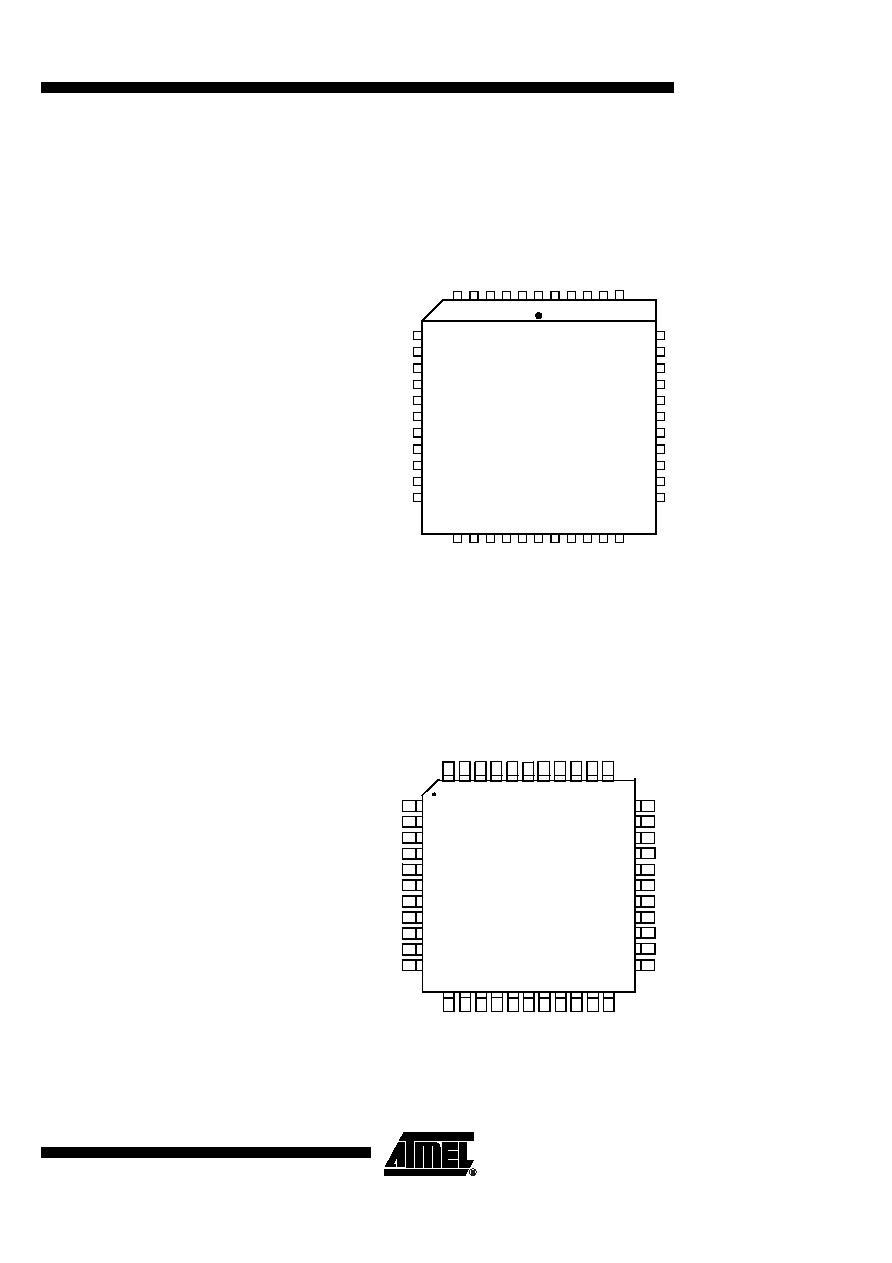
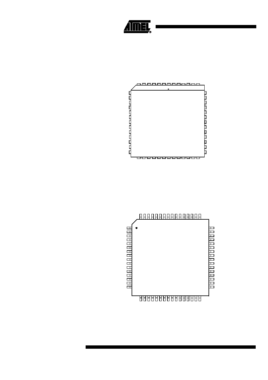
Packages: VQFP44, PLCC44, VQFP64, PLCC52
Description
The AT89C51AC3 is a high performance Flash version of the 80C51 single chip 8-bit
microcontrollers.
In X2 mode a maximum external clock rate of 20 MHz reaches a 300 ns cycle time.
Besides the AT89C51AC3 provides 64K Bytes of Flash memory including In-System
Programming (ISP) and IAP, 2K Bytes Boot Flash Memory, 2K Bytes EEPROM and
2048 byte ERAM.
Primary attention is paid to the reduction of the electro-magnetic emission of
AT89C51AC3.
Enhanced 8-bit
Microcontroller
with 64KB Flash
Memory
AT89C51AC3
5
AT89C51AC3
4383A�8051�10/04
Pin Name
Type
Description
VSS
GND
Circuit ground
TESTI
I
Must be connected to VSS
VCC
Supply Voltage
VAREF
Reference Voltage for ADC
VAGND
Reference Ground for ADC
P0.0:7
I/O
Port 0:
Is an 8-bit open drain bi-directional I/O port. Port 0 pins that have 1's written to them float, and in this state can be used as
high-impedance inputs. Port 0 is also the multiplexed low-order address and data bus during accesses to external Program
and Data Memory. In this application it uses strong internal pull-ups when emitting 1's.
Port 0 also outputs the code Bytes during program validation. External pull-ups are required during program verification.
P1.0:7
I/O
Port 1:
Is an 8-bit bi-directional I/O port with internal pull-ups. Port 1 pins can be used for digital input/output or as analog inputs for
the Analog Digital Converter (ADC). Port 1 pins that have 1's written to them are pulled high by the internal pull-up transistors
and can be used as inputs in this state. As inputs, Port 1 pins that are being pulled low externally will be the source of current
(I
IL
, see section "Electrical Characteristic") because of the internal pull-ups. Port 1 pins are assigned to be used as analog
inputs via the ADCCF register (in this case the internal pull-ups are disconnected).
As a secondary digital function, port 1 contains the Timer 2 external trigger and clock input; the PCA external clock input and
the PCA module I/O.
P1.0/AN0/T2
Analog input channel 0,
External clock input for Timer/counter2.
P1.1/AN1/T2EX
Analog input channel 1,
Trigger input for Timer/counter2.
P1.2/AN2/ECI
Analog input channel 2,
PCA external clock input.
P1.3/AN3/CEX0
Analog input channel 3,
PCA module 0 Entry of input/PWM output.
P1.4/AN4/CEX1
Analog input channel 4,
PCA module 1 Entry of input/PWM output.
P1.5/AN5/CEX2
Analog input channel 5,
PCA module 2 Entry of input/PWM output.
P1.6/AN6/CEX3
Analog input channel 6,
PCA module 3 Entry of input/PWM output.
P1.7/AN7/CEX4
Analog input channel 7,
PCA module 4 Entry ot input/PWM output.
Port 1 receives the low-order address byte during EPROM programming and program verification.
It can drive CMOS inputs without external pull-ups.
P2.0:7
I/O
Port 2:
Is an 8-bit bi-directional I/O port with internal pull-ups. Port 2 pins that have 1's written to them are pulled high by the internal
pull-ups and can be used as inputs in this state. As inputs, Port 2 pins that are being pulled low externally will be a source of
current (I
IL
, see section "Electrical Characteristic") because of the internal pull-ups. Port 2 emits the high-order address byte
during accesses to the external Program Memory and during accesses to external Data Memory that uses 16-bit addresses
(MOVX @DPTR). In this application, it uses strong internal pull-ups when emitting 1's. During accesses to external Data
Memory that use 8 bit addresses (MOVX @Ri), Port 2 transmits the contents of the P2 special function register.
It also receives high-order addresses and control signals during program validation.
It can drive CMOS inputs without external pull-ups.