Rev. 4182I≠CAN≠06/05
Features
∑
80C51 Core Architecture
∑
256 Bytes of On-chip RAM
∑
2048 Bytes of On-chip ERAM
∑
64K Bytes of On-chip Flash Memory
≠ Data Retention: 10 Years at 85∞C
≠ Read/Write Cycle: 100K
∑
2K Bytes of On-chip Flash for Bootloader
∑
2K Bytes of On-chip EEPROM
Read/Write Cycle: 100K
∑
Integrated Power Monitor (POR: PFD) To Supervise Internal Power Supply
∑
14-sources 4-level Interrupts
∑
Three 16-bit Timers/Counters
∑
Full Duplex UART Compatible 80C51
∑
High-speed Architecture
≠ In Standard Mode:
40 MHz (Vcc 3V to 5.5V, both Internal and external code execution)
60 MHz (Vcc 4.5V to 5.5V and Internal Code execution only)
≠ In X2 mode (6 Clocks/machine cycle)
20 MHz (Vcc 3V to 5.5V, both Internal and external code execution)
30 MHz (Vcc 4.5V to 5.5V and Internal Code execution only)
∑
Five Ports: 32 + 4 Digital I/O Lines
∑
Five-channel 16-bit PCA with
≠ PWM (8-bit)
≠ High-speed Output
≠ Timer and Edge Capture
∑
Double Data Pointer
∑
21-bit WatchDog Timer (7 Programmable Bits)
∑
A 10-bit Resolution Analog to Digital Converter (ADC) with 8 Multiplexed Inputs
∑
SPI Interface, (PLCC52, VPFP64 and CABGA 64 packages only)
∑
Full CAN Controller
≠ Fully Compliant with CAN Rev 2.0A and 2.0B
≠ Optimized Structure for Communication Management (Via SFR)
≠ 15 Independent Message Objects
≠ Each Message Object Programmable on Transmission or Reception
≠ Individual Tag and Mask Filters up to 29-bit Identifier/Channel
≠ 8-byte Cyclic Data Register (FIFO)/Message Object
≠ 16-bit Status and Control Register/Message Object
≠ 16-bit Time-Stamping Register/Message Object
≠ CAN Specification 2.0 Part A or 2.0 Part B Programmable for Each Message
Object
≠ Access to Message Object Control and Data Registers Via SFR
≠ Programmable Reception Buffer Length Up To 15 Message Objects
≠ Priority Management of Reception of Hits on Several Message Objects at the
Same Time (Basic CAN Feature)
≠ Priority Management for Transmission
≠ Message Object Overrun Interrupt
≠ Supports
≠ Time Triggered Communication
≠ Autobaud and Listening Mode
≠ Programmable Automatic Reply Mode
≠ 1-Mbit/s Maximum Transfer Rate at 8 MHz
(1)
Crystal Frequency in X2 Mode
≠ Readable Error Counters
≠ Programmable Link to On-chip Timer for Time Stamping and Network
Synchronization
≠ Independent Baud Rate Prescaler
≠ Data, Remote, Error and Overload Frame Handling
1.
At BRP = 1 sampling point will be fixed.
Enhanced 8-bit
MCU with CAN
Controller and
Flash Memory
AT89C51CC03
2
AT89C51CC03
4182I≠CAN≠06/05
∑
On-chip Emulation Logic (Enhanced Hook System)
∑
Power Saving Modes
≠ Idle Mode
≠ Power-down Mode
∑
Power Supply: 3 volts to 5.5 volts
∑
Temperature Range: Industrial (-40
∞ to +85∞C), Automotive (-40∞C to +125∞C)
∑
Packages: VQFP44, PLCC44, VQFP64, PLCC52, CA-BGA64
Description
The AT89C51CC03 is a member of the family of 8-bit microcontrollers dedicated to CAN
network applications.
In X2 mode a maximum external clock rate of 20 MHz reaches a 300 ns cycle time.
Besides the full CAN controller AT89C51CC03 provides 64K Bytes of Flash memory
including In-System Programming (ISP), 2K Bytes Boot Flash Memory, 2K Bytes
EEPROM and 2048 byte ERAM.
Primary attention is paid to the reduction of the electro-magnetic emission of
AT89C51CC03.
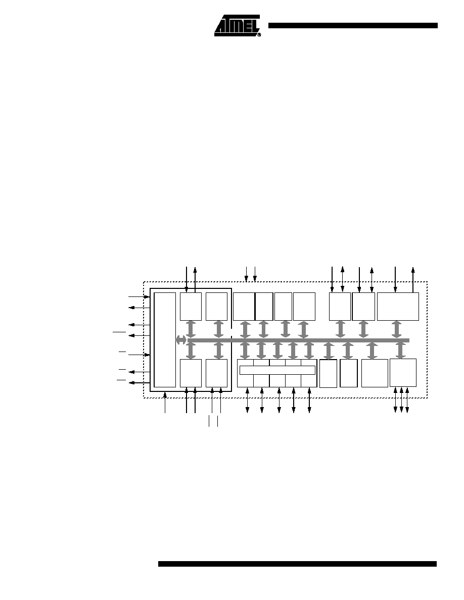
Block Diagram
Notes: 1. 8 analog Inputs/8 Digital I/O
2. 5-Bit I/O Port
Timer 0
INT
RAM
256x8
T0
T1
Rx
D
TxD
WR
RD
EA
PSEN
ALE
XTAL2
XTAL1
UART
CPU
Timer 1
INT1
Ctrl
INT0
C51
CORE
Port 0
P0
Port 1 Port 2 Port 3
Parallel I/O Ports and Ext. Bus
P1
(1
)
P2
P3
ERAM
2048
IB-bus
PCA
RESE
T
Watch
Dog
PCA
ECI
Vs
s
Vc
c
Timer2
T2EX
T2
Port 4
P4
(2)
Emul
Unit
10 bit
ADC
Flash
64k x 8
Boot
loader
2kx8
EE
PROM
2kx8
CAN
CONTROLLER
TxDC
RxDC
SPI
Interface
MO
SI
SC
K
MI
SO
3
AT89C51CC03
4182I≠CAN≠06/05
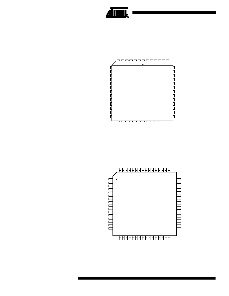
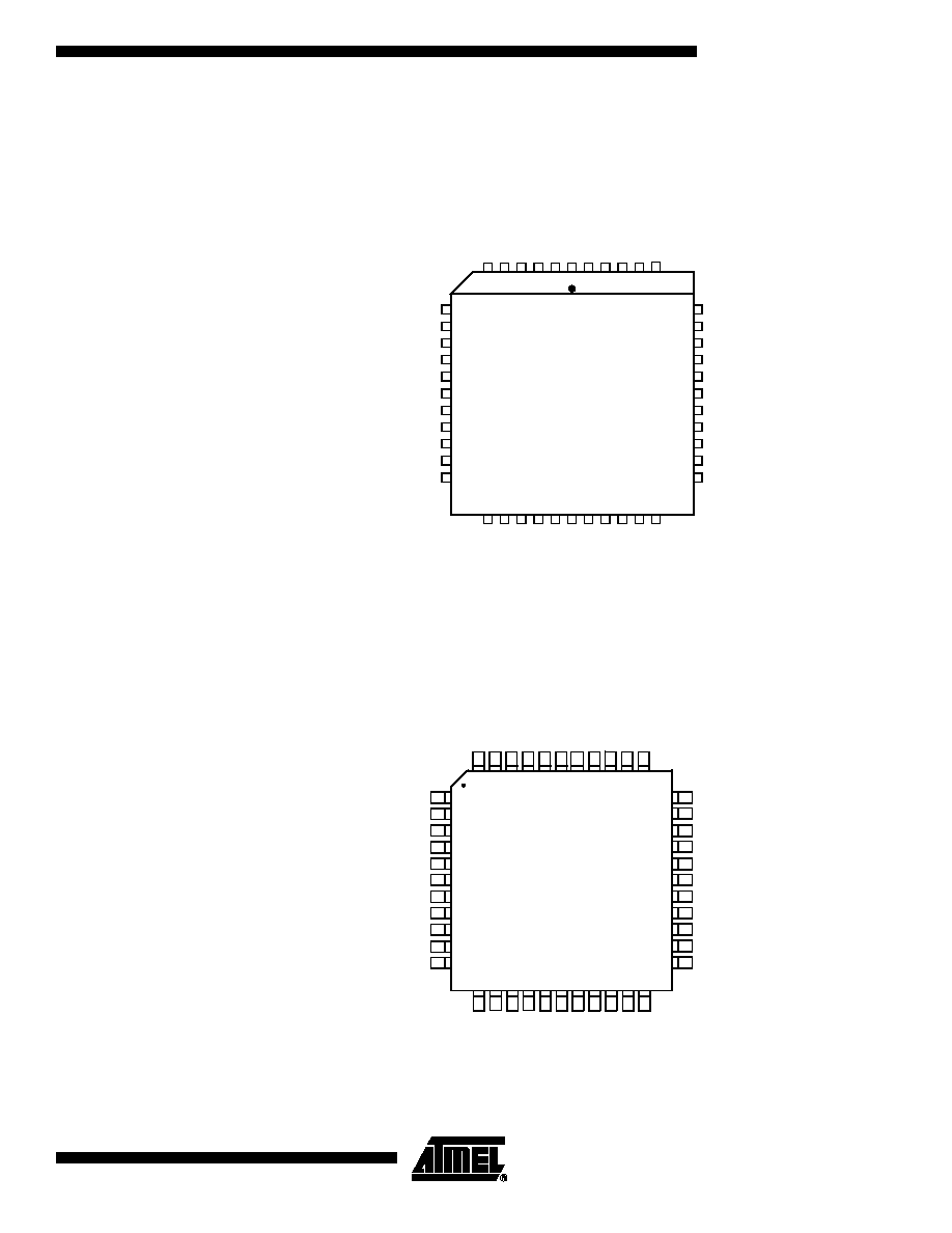
Pin Configuration
PLCC44
P1.3/AN3/C
EX
0
P1.2/AN2/EC
I
P1.1/AN1/T
2EX
P1.0/AN 0/T
2
VAREF
VAG
N
D
RESET
VS
S
VCC
XTAL1
XTAL2
P3.7
/RD
P4.0/ T
x
DC
P4.1/Rx
D
C
P2.7
/A15
P2.6
/A14
P2.5
/A13
P2.4
/A12
P2.3
/A11
P2.2
/A10
P
2
.1/A9
P3.6/WR
39
38
37
36
35
34
33
32
29
30
31
7
8
9
10
11
12
13
14
17
16
15
18
19
20
21
22
23
24
25
26
27
28
6
5
4
3
2
44
43
42
41
40
ALE
PSEN
P0.7/AD7
P0.6/AD6
P0.5/AD5
P0.2/AD2
P0.3/AD3
P0.4/AD4
P0.1/AD1
P0.0/AD0
P2.0/A8
P1.4/AN4/CEX1
P1.5/AN5/CEX2
P1.6/AN6/CEX3
P1.7/AN7/CEX4
EA
P3.0/RxD
P3.1/TxD
P3.2/INT0
P3.3/INT1
P3.4/T0
P3.5/T1
1
43 42 41 40 39
44
38 37 36 35 34
12 13
17
16
15
14
20
19
18
21 22
33
32
31
30
29
28
27
26
25
24
23
VQFP44
1
2
3
4
5
6
7
8
9
10
11
P1.4/AN4/CEX1
P1.5/AN5/CEX2
P1.6/AN6/CEX3
P1.7/AN7/CEX4
EA
P3.0/RxD
P3.1/TxD
P3.2/INT0
P3.3/INT1
P3.4/T0
P3.5/T1
ALE
PSEN
P0.7/AD7
P0.6/AD6
P0.5/AD5
P0.2 /AD2
P0.3 /AD3
P0.4 /AD4
P0.1 /AD1
P0.0 /AD0
P2.0/A8
P
1
.3/AN3/C
E
X
0
P
1
.2/AN2/ECI
P
1
.1/AN1/T
2EX
P
1
.0/AN 0/T
2
VA
RE
F
VA
GN
D
RESE
T
VS
S
VC
C
XT
AL
1
XT
AL
2
P
3
.7/RD
P4.0/T
xDC
P4.1/R
xDC
P
2
.7/A15
P
2
.6/A14
P
2
.5/A13
P
2
.4/A12
P
2
.3/A11
P
2
.2/A10
P2.1/A9
P3.6/WR