4289B�8051�12/03
1
Features
�
80C52 Compatible
� 8051 Instruction Compatible
� Six 8-bit I/O Ports (64 pins or 68 Pins Versions)
� Four 8-bit I/O Ports (44 Pins Version)
� Three 16-bit Timer/Counters
� 256 bytes Scratch Pad RAM
� 10 Interrupt Sources With 4 Priority Levels
�
ISP (In-System Programming) Using Standard V
CC
Power Supply
�
Integrated Power Monitor (POR/PFD) to Supervise Internal Power Supply
�
Boot ROM Contains Low Level Flash Programming Routines and a Default Serial
Loader
�
High-speed Architecture
� In Standard Mode:
40 MHz (Vcc 2.7V to 5.5V, Both Internal and External Code Execution)
60 MHz (Vcc 4.5V to 5.5V and Internal Code Execution Only)
� In X2 Mode (6 Clocks/Machine Cycle)
20 MHz (Vcc 2.7V to 5.5V, Both Internal and External Code Execution)
30 MHz (Vcc 4.5V to 5.5V and Internal Code Execution Only)
�
64K bytes On-chip Flash Program/Data Memory
� Byte and Page (128 bytes) Erase and Write
� 100k Write Cycles
�
On-chip 1792 bytes Expanded RAM (XRAM)
� Software Selectable Size (0, 256, 512, 768, 1024, 1792 bytes)
� 768 bytes Selected at Reset for T89C51RD2 Compatibility
�
On-chip 2048 bytes EEPROM block for Data Storage
� 100k Write Cycles
�
Dual Data Pointer
�
32 KHz Crystal Oscillator
�
Variable Length MOVX for Slow RAM/Peripherals
�
Improved X2 Mode with Independant Selection for CPU and Each Peripheral
�
Keyboard Interrupt Interface on Port 1
�
SPI Interface (Master/Slave Mode)
�
8-bit Clock Prescaler
�
Two Wire Interface 400K bit/s
�
Programmable Counter Array with:
� High Speed Output
� Compare/Capture
� Pulse Width Modulator
� Watchdog Timer Capabilities
�
Asynchronous Port Reset
�
Full Duplex Enhanced UART with Dedicated Internal Baud Rate Generator
�
Low EMI (inhibit ALE)
�
Hardware Watchdog Timer (One-time Enabled with Reset-Out), Power-Off Flag
�
Power Control Modes: Idle Mode, Power-down Mode
�
Power Supply: 2.7V to 5.5V
�
Temperature Ranges: Industrial (-40 to +85
�
C)
�
Packages: PLCC44, VQFP44
Description
AT89C51ID2 is a high performance CMOS Flash version of the 80C51 CMOS single
chip 8-bit microcontroller. It contains a 64 Kbytes Flash memory block for program
and for data.
The 64 Kbytes Flash memory can be programmed either in parallel mode or in serial
mode with the ISP capability or with software. The programming voltage is internally
generated from the standard V
CC
pin.
8-bit Flash
Microcontroller
AT89C51ID2
2
AT89C51ID2
4289B�8051�12/03
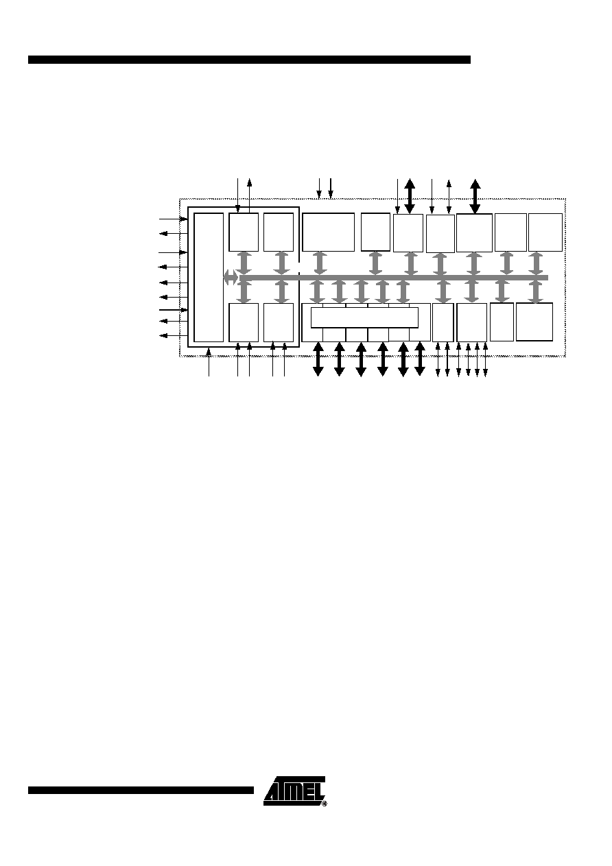
The AT89C51ID2 retains all features of the Atmel 80C52 with 256 bytes of internal
RAM, a 10-source 4-level interrupt controller and three timer/counters.
In addition, the AT89C51ID2 has a Programmable Counter Array, an XRAM of 1792
bytes, a Hardware Watchdog Timer, SPI and Keyboard, a more versatile serial channel
that facilitates multiprocessor communication (EUART) and a speed improvement
mechanism (X2 mode).
The fully static design of the AT89C51ID2 allows to reduce system power consumption
by bringing the clock frequency down to any value, even DC, without loss of data.
The AT89C51ID2 has 2 software-selectable modes of reduced activity and 8-bit clock
prescaler for further reduction in power consumption. In the Idle mode the CPU is frozen
while the peripherals and the interrupt system are still operating. In the power-down
mode the RAM is saved and all other functions are inoperative.
The added features of the AT89C51ID2 make it more powerful for applications that need
pulse width modulation, high speed I/O and counting capabilities such as alarms, motor
control, corded phones, smart card readers.
Table 1. Memory Size and I/O pins
AT89C51ID2
Flash (bytes)
XRAM (bytes)
TOTAL RAM
(bytes)
I/O
PLCC44/VQFP44
64K
1792
2048
34

4
AT89C51ID2
4289B�8051�12/03
SFR Mapping
The Special Function Registers (SFRs) of the AT89C51ID2 fall into the following
categories:
�
C51 core registers: ACC, B, DPH, DPL, PSW, SP
�
I/O port registers: P0, P1, P2, P3, PI2
�
Timer registers: T2CON, T2MOD, TCON, TH0, TH1, TH2, TMOD, TL0, TL1, TL2,
RCAP2L, RCAP2H
�
Serial I/O port registers: SADDR, SADEN, SBUF, SCON
�
PCA (Programmable Counter Array) registers: CCON, CCAPMx, CL, CH, CCAPxH,
CCAPxL (x: 0 to 4)
�
Power and clock control registers: PCON
�
Hardware Watchdog Timer registers: WDTRST, WDTPRG
�
Interrupt system registers: IE0, IPL0, IPH0, IE1, IPL1, IPH1
�
Keyboard Interface registers: KBE, KBF, KBLS
�
SPI registers: SPCON, SPSTR, SPDAT
�
2-wire Interface registers: SSCON, SSCS, SSDAT, SSADR
�
BRG (Baud Rate Generator) registers: BRL, BDRCON
�
Flash register: FCON
�
Clock Prescaler register: CKRL
�
32 kHz Sub Clock Oscillator registers: CKSEL, OSSCON
�
Others: AUXR, AUXR1, CKCON0, CKCON1
5
AT89C51ID2
4289B�8051�12/03
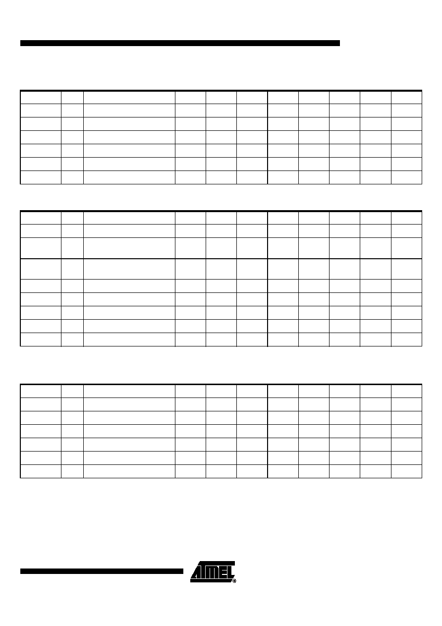
Table 2. C51 Core SFRs
Mnemonic
Add
Name
7
6
5
4
3
2
1
0
ACC
E0h
Accumulator
B
F0h
B Register
PSW
D0h
Program Status Word
CY
AC
F0
RS1
RS0
OV
F1
P
SP
81h
Stack Pointer
DPL
82h
Data Pointer Low byte
DPH
83h
Data Pointer High byte
Table 3. System Management SFRs
Mnemonic
Add
Name
7
6
5
4
3
2
1
0
PCON
87h
Power Control
SMOD1
SMOD0
-
POF
GF1
GF0
PD
IDL
AUXR
8Eh
Auxiliary Register 0
-
-
M0
XRS1
XRS0
EXTRA
M
AO
AUXR1
A2h
Auxiliary Register 1
-
-
ENBOO
T
-
GF3
0
-
DPS
CKRL
97h
Clock Reload Register
-
-
-
-
-
-
-
-
CKSEL
85h
Clock Selection Register
-
-
-
-
-
-
-
CKS
OSCON
86h
Oscillator Control Register
-
-
-
-
-
SCLKT0
OscBEn
OscAEn
CKCKON0
8Fh
Clock Control Register 0
TWIX2
WDTX2
PCAX2
SIX2
T2X2
T1X2
T0X2
X2
CKCKON1
AFh
Clock Control Register 1
-
-
-
-
-
-
-
SPIX2
Table 4. Interrupt SFRs
Mnemonic
Add
Name
7
6
5
4
3
2
1
0
IEN0
A8h
Interrupt Enable Control 0
EA
EC
ET2
ES
ET1
EX1
ET0
EX0
IEN1
B1h
Interrupt Enable Control 1
-
-
-
-
-
ESPI
ETWI
EKBD
IPH0
B7h
Interrupt Priority Control High 0
-
PPCH
PT2H
PSH
PT1H
PX1H
PT0H
PX0H
IPL0
B8h
Interrupt Priority Control Low 0
-
PPCL
PT2L
PSL
PT1L
PX1L
PT0L
PX0L
IPH1
B3h
Interrupt Priority Control High 1
-
-
-
-
-
SPIH
IE2CH
KBDH
IPL1
B2h
Interrupt Priority Control Low 1
-
-
-
-
-
SPIL
IE2CL
KBDL