Rev. 4180B≠8051≠04/03
Features
∑
80C52 Compatible
≠ 8051 Pin and Instruction Compatible
≠ Four 8-bit I/O Ports
≠ Three 16-bit Timer/Counters
≠ 256 Bytes Scratch Pad RAM
≠ 9 Interrupt Sources with 4 Priority Levels
≠ Dual Data Pointer
∑
Variable Length MOVX for Slow RAM/Peripherals
∑
ISP (In-system Programming) Using Standard V
CC
Power Supply
∑
Boot ROM Contains Low Level Flash Programming Routines and a Default Serial
Loader
∑
High-speed Architecture
≠ 48 MHz in Standard Mode and Internal Code Execution (40 MHz for external code)
≠ 24 MHz in X2 Mode and internal code execution (20 MHz for external code)
≠ 16K/32K Bytes On-chip Flash Program/Data Memory
≠ Byte and Page (128 Bytes) Erase and Write
≠ 100K Write Cycles
∑
On-chip 1024 Bytes Expanded RAM (XRAM)
≠ Software Selectable Size (0, 256, 512, 768, 1024 Bytes)
≠ 256 Bytes Selected at Reset for TS87C51RB2/RC2 Compatibility
∑
Keyboard Interrupt Interface on Port P1
∑
SPI Interface (Master/Slave Mode)
∑
8-bit Clock Prescaler
∑
Improved X2 Mode with Independent Selection for CPU and Each Peripheral
∑
Programmable Counter Array 5 Channels
≠
High-speed Output
≠
Compare/Capture
≠
Pulse Width Modulator
≠
Watchdog Timer Capabilities
∑
Asynchronous Port Reset
∑
Full Duplex Enhanced UART
∑
Dedicated Baud Rate Generator for UART
∑
Low EMI (Inhibit ALE)
∑
Hardware Watchdog Timer (One-time Enabled with Reset-out)
∑
Power Control Modes
≠ Idle Mode
≠ Power-down Mode
≠ Power-off Flag
∑
Power Supply:
≠ 2.7 to 3.6 (3V Version)
≠ 2.7 to 5.5V (5V Version)
∑
Temperature Ranges: Commercial (0 to +70
∞
C) and Industrial (-40
∞
C to +85
∞
C)
∑
Packages: PDIL40, PLCC44, VQFP44
Description
The AT89C51RB2/RC2 is a high-performance Flash version of the 80C51 8-bit micro-
controllers. It contains a 16K or 32K Bytes Flash memory block for program and data.
The Flash memory can be programmed either in parallel mode or in serial mode with
the ISP capability or with software. The programming voltage is internally generated
from the standard VCC pin.
The AT89C51RB2/RC2 retains all features of the 80C52 with 256 Bytes of internal
RAM, a 9-source 4-level interrupt controller and three timer/counters.
8-bit
Microcontroller
with 16K/
32K Bytes Flash
AT89C51RB2
AT89C51RC2
2
AT89C51RB2/RC2
4180B≠8051≠04/03
In addition, the AT89C51RB2/RC2 has a Programmable Counter Array, an XRAM of
1024 Bytes, a Hardware Watchdog Timer, a Keyboard Interface, an SPI Interface, a
more versatile serial channel that facilitates multiprocessor communication (EUART)
and a speed improvement mechanism (X2 mode).
The Pinout is the standard 40/44 pins of the C52.
The fully static design reduces system power consumption of the AT89C51RB2/RC2 by
allowing it to bring the clock frequency down to any value, even DC, without loss of data.
The AT89C51RB2/RC2 has 2 software-selectable modes of reduced activity and 8-bit
clock prescaler for further reduction in power consumption. In Idle mode, the CPU is fro-
zen while the peripherals and the interrupt system are still operating. In power-down
mode, the RAM is saved and all other functions are inoperative.
The added features of the AT89C51RB2/RC2 make it more powerful for applications
that need pulse width modulation, high speed I/O and counting capabilities such as
alarms, motor control, corded phones, and smart card readers.
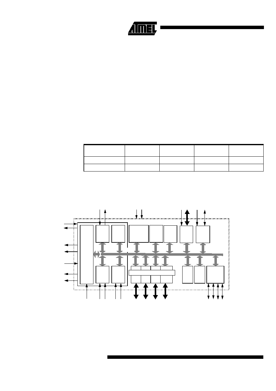
Block Diagram
Figure 1. Block Diagram
Notes:
1. Alternate function of Port 1.
2. Alternate function of Port 3.
Table 1. Memory Size
Part Number
Flash (Bytes)
XRAM (Bytes)
TOTAL RAM
(Bytes)
I/O
AT89C51RB2
16K
1024
1280
32
AT89C51RC2
32K
1024
1280
32
Timer 0
INT
RAM
256x8
T0
T1
Rx
D
Tx
D
WR
RD
EA
PSEN
ALE/
XTAL2
XTAL1
EUART
CPU
Timer 1
INT
1
Ctrl
INT
0
(2)
(2)
C51
CORE
(2) (2)
(2) (2)
Port 0
P0
Port 1 Port 2 Port 3
Parallel I/O Ports & Ext. Bus
P1
P2
P3
XRAM
1Kx8
IB-bus
PCA
RESET
PROG
Watch
Dog
PCA
ECI
Vs
s
V
CC
(2)
(2)
(1)
(1)
Timer2
T2
EX
T2
(1)
(1)
Flash
32Kx8 or
16Kx8
Key
Board
ROM
2Kx8
Boot
+
BRG
SPI
MI
S
O
MO
S
I
SCK
(1) (1) (1)
SS
(1)

3
AT89C51RB2/RC2
4180B≠8051≠04/03
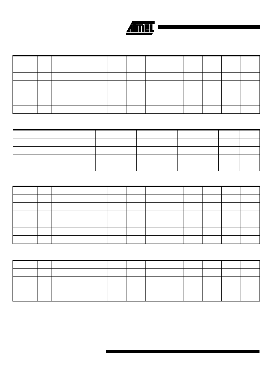
SFR Mapping
The Special Function Registers (SFRs) of the AT89C51RB2/RC2 fall into the following
categories:
∑
C51 core registers: ACC, B, DPH, DPL, PSW, SP
∑
I/O port registers: P0, P1, P2, P3
∑
Timer registers: T2CON, T2MOD, TCON, TH0, TH1, TH2, TMOD, TL0, TL1, TL2,
RCAP2L, RCAP2H
∑
Serial I/O port registers: SADDR, SADEN, SBUF, SCON
∑
PCA (Programmable Counter Array) registers: CCON, CCAPMx, CL, CH, CCAPxH,
CCAPxL (x: 0 to 4)
∑
Power and clock control registers: PCON
∑
Hardware Watchdog Timer registers: WDTRST, WDTPRG
∑
Interrupt system registers: IEN0, IPL0, IPH0, IEN1, IPL1, IPH1
∑
Keyboard Interface registers: KBE, KBF, KBLS
∑
SPI registers: SPCON, SPSTR, SPDAT
∑
BRG (Baud Rate Generator) registers: BRL, BDRCON
∑
Flash register: FCON
∑
Clock Prescaler register: CKRL
∑
Others: AUXR, AUXR1, CKCON0, CKCON1
4
AT89C51RB2/RC2
4180B≠8051≠04/03
Table 2. C51 Core SFRs
Mnemonic
Add
Name
7
6
5
4
3
2
1
0
ACC
E0h
Accumulator
B
F0h
B Register
PSW
D0h
Program Status Word
CY
AC
F0
RS1
RS0
OV
F1
P
SP
81h
Stack Pointer
DPL
82h
Data Pointer Low Byte
DPH
83h
Data Pointer High Byte
Table 3. System Management SFRs
Mnemonic
Add
Name
7
6
5
4
3
2
1
0
PCON
87h
Power Control
SMOD1
SMOD0
-
-
GF1
GF0
PD
IDL
AUXR
8Eh
Auxiliary Register 0
DPU
-
M0
XRS2
XRS1
XRS0
EXTRAM
AO
AUXR1
A2h
Auxiliary Register 1
-
-
ENBOOT
-
GF3
0
-
DPS
CKRL
85h
Clock Reload Register
CKRL7
CKRL6
CKRL5
CKRL4
CKRL3
CKRL2
CKRL1
CKRL0
Table 4. Interrupt SFRs
Mnemonic
Add
Name
7
6
5
4
3
2
1
0
IEN0
A8h
Interrupt Enable Control 0
EA
EC
ET2
ES
ET1
EX1
ET0
EX0
IEN1
B1h
Interrupt Enable Control 1
-
-
-
-
-
ESPI
EI2C
KBD
IPH0
B7h
Interrupt Priority Control High 0
-
PPCH
PT2H
PHS
PT1H
PX1H
PT0H
PX0H
IPL0
B8h
Interrupt Priority Control Low 0
-
PPCL
PT2L
PLS
PT1L
PX1L
PT0L
PX0L
IPH1
B3h
Interrupt Priority Control High 1
-
-
-
-
-
SPIH
IE2CH
KBDH
IPL1
B2h
Interrupt Priority Control Low 1
-
-
-
-
-
SPIL
IE2CL
KBDL
Table 5. Port SFRs
Mnemonic
Add
Name
7
6
5
4
3
2
1
0
P0
80h
8-bit Port 0
P1
90h
8-bit Port 1
P2
A0h
8-bit Port 2
P3
B0h
8-bit Port 3
5
AT89C51RB2/RC2
4180B≠8051≠04/03
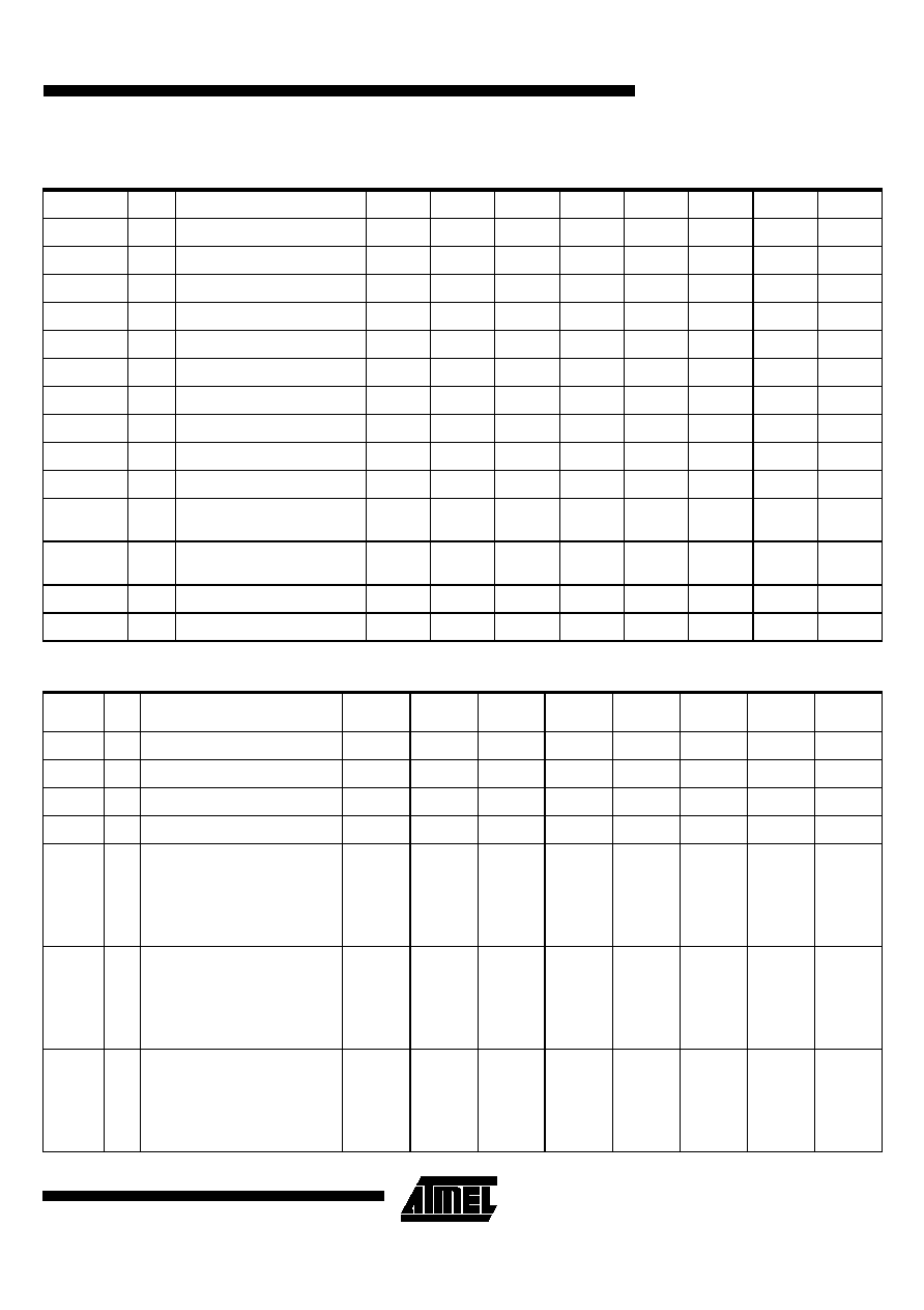
Table 6. Timer SFRs
Mnemonic
Add
Name
7
6
5
4
3
2
1
0
TCON
88h
Timer/Counter 0 and 1 Control
TF1
TR1
TF0
TR0
IE1
IT1
IE0
IT0
TMOD
89h
Timer/Counter 0 and 1 Modes
GATE1
C/T1#
M11
M01
GATE0
C/T0#
M10
M00
TL0
8Ah
Timer/Counter 0 Low Byte
TH0
8Ch
Timer/Counter 0 High Byte
TL1
8Bh
Timer/Counter 1 Low Byte
TH1
8Dh
Timer/Counter 1 High Byte
WDTRST
A6h
Watchdog Timer Reset
WDTPRG
A7h
Watchdog Timer Program
-
-
-
-
-
WTO2
WTO1
WTO0
T2CON
C8h
Timer/Counter 2 control
TF2
EXF2
RCLK
TCLK
EXEN2
TR2
C/T2#
CP/RL2#
T2MOD
C9h
Timer/Counter 2 Mode
-
-
-
-
-
-
T2OE
DCEN
RCAP2H
CBh
Timer/Counter 2 Reload/Capture
High Byte
RCAP2L
CAh
Timer/Counter 2 Reload/Capture
Low Byte
TH2
CDh
Timer/Counter 2 High Byte
TL2
CCh
Timer/Counter 2 Low Byte
Table 7. PCA SFRs
Mnemo-
nic
Add
Name
7
6
5
4
3
2
1
0
CCON
D8h
PCA Timer/Counter Control
CF
CR
-
CCF4
CCF3
CCF2
CCF1
CCF0
CMOD
D9h
PCA Timer/Counter Mode
CIDL
WDTE
-
-
-
CPS1
CPS0
ECF
CL
E9h
PCA Timer/Counter Low Byte
CH
F9h
PCA Timer/Counter High Byte
CCAPM0
CCAPM1
CCAPM2
CCAPM3
CCAPM4
DAh
DBh
DCh
DDh
DEh
PCA Timer/Counter Mode 0
PCA Timer/Counter Mode 1
PCA Timer/Counter Mode 2
PCA Timer/Counter Mode 3
PCA Timer/Counter Mode 4
-
ECOM0
ECOM1
ECOM2
ECOM3
ECOM4
CAPP0
CAPP1
CAPP2
CAPP3
CAPP4
CAPN0
CAPN1
CAPN2
CAPN3
CAPN4
MAT0
MAT1
MAT2
MAT3
MAT4
TOG0
TOG1
TOG2
TOG3
TOG4
PWM0
PWM1
PWM2
PWM3
PWM4
ECCF0
ECCF1
ECCF2
ECCF3
ECCF4
CCAP0H
CCAP1H
CCAP2H
CCAP3H
CCAP4H
FAh
FBh
FCh
FDh
FEh
PCA Compare Capture Module 0 H
PCA Compare Capture Module 1 H
PCA Compare Capture Module 2 H
PCA Compare Capture Module 3 H
PCA Compare Capture Module 4 H
CCAP0H7
CCAP1H7
CCAP2H7
CCAP3H7
CCAP4H7
CCAP0H6
CCAP1H6
CCAP2H6
CCAP3H6
CCAP4H6
CCAP0H5
CCAP1H5
CCAP2H5
CCAP3H5
CCAP4H5
CCAP0H4
CCAP1H4
CCAP2H4
CCAP3H4
CCAP4H4
CCAP0H3
CCAP1H3
CCAP2H3
CCAP3H3
CCAP4H3
CCAP0H2
CCAP1H2
CCAP2H2
CCAP3H2
CCAP4H2
CCAP0H1
CCAP1H1
CCAP2H1
CCAP3H1
CCAP4H1
CCAP0H0
CCAP1H0
CCAP2H0
CCAP3H0
CCAP4H0
CCAP0L
CCAP1L
CCAP2L
CCAP3L
CCAP4L
EAh
EBh
ECh
EDh
EEh
PCA Compare Capture Module 0 L
PCA Compare Capture Module 1 L
PCA Compare Capture Module 2 L
PCA Compare Capture Module 3 L
PCA Compare Capture Module 4 L
CCAP0L7
CCAP1L7
CCAP2L7
CCAP3L7
CCAP4L7
CCAP0L6
CCAP1L6
CCAP2L6
CCAP3L6
CCAP4L6
CCAP0L5
CCAP1L5
CCAP2L5
CCAP3L5
CCAP4L5
CCAP0L4
CCAP1L4
CCAP2L4
CCAP3L4
CCAP4L4
CCAP0L3
CCAP1L3
CCAP2L3
CCAP3L3
CCAP4L3
CCAP0L2
CCAP1L2
CCAP2L2
CCAP3L2
CCAP4L2
CCAP0L1
CCAP1L1
CCAP2L1
CCAP3L1
CCAP4L1
CCAP0L0
CCAP1L0
CCAP2L0
CCAP3L0
CCAP4L0