1
Features
∑
High-density, High-performance, Electrically-erasable Complex Programmable
Logic Device
≠ 64 Macrocells
≠ 5 Product Terms per Macrocell, Expandable up to 40 per Macrocell
≠ 44, 68, 84, 100 Pins
≠ 7.5 ns Maximum Pin-to-pin Delay
≠ Registered Operation up to 125 MHz
≠ Enhanced Routing Resources
∑
In-System Programmability (ISP) via JTAG
∑
Flexible Logic Macrocell
≠ D/T/Latch Configurable Flip-flops
≠ Global and Individual Register Control Signals
≠ Global and Individual Output Enable
≠ Programmable Output Slew Rate
≠ Programmable Output Open Collector Option
≠ Maximum Logic Utilization by Burying a Register with a COM Output
∑
Advanced Power Management Features
≠ Automatic µA Standby for "L" Version
≠ Pin-controlled 1 mA Standby Mode
≠ Programmable Pin-keeper Circuits on Inputs and I/Os
≠ Reduced-power Feature per Macrocell
∑
Available in Commercial and Industrial Temperature Ranges
∑
Available in 44-, 68-, and 84-lead PLCC; 44- and 100-lead TQFP; and 100-lead PQFP
∑
Advanced EE Technology
≠ 100% Tested
≠ Completely Reprogrammable
≠ 10,000 Program/Erase Cycles
≠ 20-year Data Retention
≠ 2000V ESD Protection
≠ 200 mA Latch-up Immunity
∑
JTAG Boundary-scan Testing to IEEE Std. 1149.1-1990 and 1149.1a-1993 Supported
∑
PCI-compliant
∑
3.3V or 5.0V I/O Pins
∑
Security Fuse Feature
Enhanced Features
∑
Improved Connectivity (Additional Feedback Routing, Alternate Input Routing)
∑
Output Enable Product Terms
∑
Transparent ≠ Latch Mode
∑
Combinatorial Output with Registered Feedback within Any Macrocell
∑
Three Global Clock Pins
∑
ITD (Input Transition Detection) Circuits on Global Clocks, Inputs and I/O
∑
Fast Registered Input from Product Term
∑
Programmable "Pin-keeper" Option
∑
V
CC
Power-up Reset Option
∑
Pull-up Option on JTAG Pins TMS and TDI
∑
Advanced Power Management Features
≠ Edge-controlled Power-down "L"
≠ Individual Macrocell Power Option
≠ Disable ITD on Global Clocks, Inputs and I/O
High-
performance
Complex
Programmable
Logic Device
ATF1504AS
ATF1504ASL
Rev. 0950N≠PLD≠07/02

4
ATF1504AS(L)
0950N≠PLD≠07/02
Description
The ATF1504AS is a high-performance, high-density complex programmable logic
device (CPLD) that utilizes Atmel's proven electrically-erasable memory technology.
With 64 logic macrocells and up to 68 inputs, it easily integrates logic from several TTL,
SSI, MSI, LSI and classic PLDs. The ATF1504AS's enhanced routing switch matrices
increase usable gate count and the odds of successful pin-locked design modifications.
The ATF1504AS has up to 68 bi-directional I/O pins and four dedicated input pins,
depending on the type of device package selected. Each dedicated pin can also serve
as a global control signal, register clock, register reset or output enable. Each of these
control signals can be selected for use individually within each macrocell.
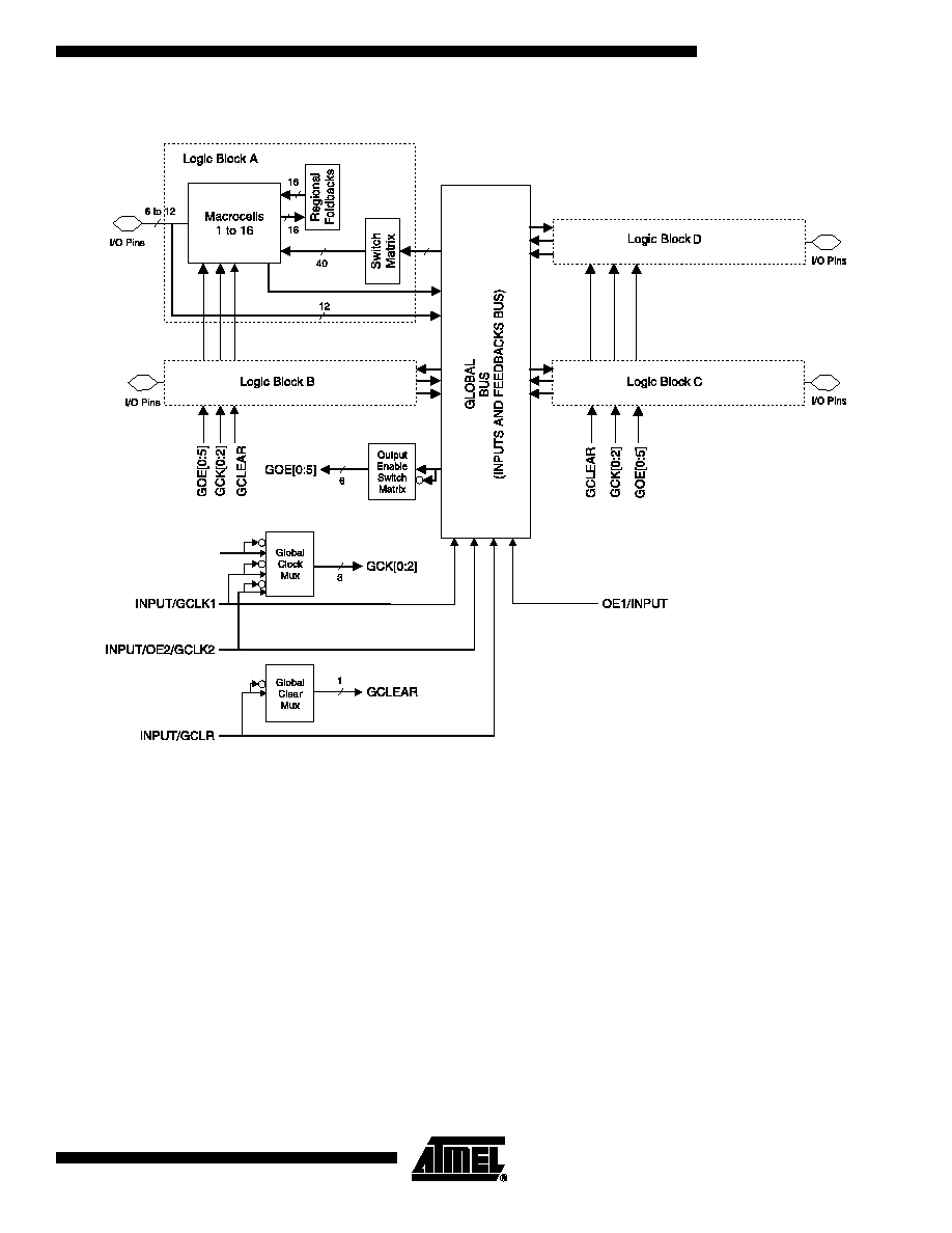
Each of the 64 macrocells generates a buried feedback that goes to the global bus.
Each input and I/O pin also feeds into the global bus. The switch matrix in each logic
block then selects 40 individual signals from the global bus. Each macrocell also gener-
ates a foldback logic term that goes to a regional bus. Cascade logic between
macrocells in the ATF1504AS allows fast, efficient generation of complex logic func-
tions. The ATF1504AS contains four such logic chains, each capable of creating sum
term logic with a fan-in of up to 40 product terms.
The ATF1504AS macrocell, shown in Figure 1, is flexible enough to support highly-com-
plex logic functions operating at high speed. The macrocell consists of five sections:
product terms and product term select multiplexer, OR/XOR/CASCADE logic, a flip-flop,
output select and enable, and logic array inputs.
5
ATF1504AS(L)
0950N≠PLD≠07/02
Block Diagram
Unused product terms are automatically disabled by the compiler to decrease power
consumption. A security fuse, when programmed, protects the contents of the
ATF1504AS. Two bytes (16 bits) of User Signature are accessible to the user for pur-
poses such as storing project name, part number, revision or date. The User Signature
is accessible regardless of the state of the security fuse.
The ATF1504AS device is an in-system programmable (ISP) device. It uses the indus-
try-standard 4-pin JTAG interface (IEEE Std. 1149.1), and is fully-compliant with JTAG's
Boundary-scan Description Language (BSDL). ISP allows the device to be programmed
without removing it from the printed circuit board. In addition to simplifying the manufac-
turing flow, ISP also allows design modifications to be made in the field via software.
I/O (MC64)/GCLK3