1
Features
∑
2nd Generation EE PROM-based Complex Programmable Logic Devices
≠ V
CCIO
of 5.0V or 3.3V with 3.3V Operation being 5V Tolerant
≠ 32 - 256 Macrocells with Enhanced Features
≠ Pin-compatible with Industry Standard Devices
≠ Speeds to 5 ns Maximum Pin-to-pin Delay
≠ Registered Operation to 250 MHz
∑
Enhanced Macrocells with Logic Doubling
TM
Features
≠ Bury Either Register or COM while Using the Other for Output
≠ Dual Independent Feedback Allows Multiple Latch Functions per Macrocell
≠ 5 Product Terms per Macrocell, expandable to 40 per Macrocell with Cascade
Logic, Plus 15 more with Foldback Logic
≠ D/T/Latch Configurable Flip-flops plus Transparent Latches
≠ Global and/or per Macrocell Register Control Signals
≠ Global and/or per Macrocell Output Enable
≠ Programmable Output Slew Rate per Macrocell
≠ Programmable Output Open Collector Option per Macrocell
≠ Fast Registered Input from Product Term
∑
Enhanced Connectivity
≠ Single Level Switch Matrix for Maximum Routing Options
≠ Up to 40 Inputs per Logic Block
∑
Advanced Power Management Features
≠ ITD (Input Transition Detection) Available Individually on Global Clocks, Inputs and
I/O for µA Level Standby Current for "L" Versions
≠ Pin-controlled 1 mA Standby Mode
≠ Reduced-power Option per Macrocell
≠ Automatic Power Down of Unused Macrocells
≠ Programmable Pin-keeper Inputs and I/Os
∑
Available in Commercial and Industrial Temperature Ranges
∑
Available in All Popular Packages Including PLCC, PQFP and TQFP
∑
EE PROM Technology
≠ 100% Tested
≠ Completely Reprogrammable
≠ 10,000 Program/Erase Cycles
≠ 20 Year Data Retention
≠ 2000V ESD Protection
≠ 200 mA Latch-up Immunity
∑
JTAG Boundary-scan Testing Port per IEEE 1149.1-1990 and 1149.1a-1993
≠ Pull-up Option on JTAG Pins TMS and TDI
∑
IEEE 1532 Compatibility for Fast In-System Programmability (ISP) via JTAG
∑
PCI-compliant
∑
Security Fuse Feature
ATF15xxSE
Family
Datasheet
ATF1502SE(L)
ATF1504SE(L)
ATF1508SE(L)
ATF1516SE(L)
Preliminary
Rev. 2401D≠PLD≠09/02

2
ATF15xxSE Family
2401D≠PLD≠09/02
General
Description
Beginning with the introduction of the 100% connected ATF1500 with 32 enhanced macrocells
in 1996, Atmel's CPLD products have delivered extra IO connectivity and logic reusability.
Atmel's commitment to efficient, flexible architecture has continued with the current Atmel
ATF15xxSE Family of industry-standard, pin-compatible CPLDs. Atmel's Logic Doubling
architecture consists of wider fan-in, additional routing and clock options, combined with
sophisticated, proprietary device fitters, extend CPLD place and route efficiency. Atmel
enhanced macrocell includes double independent buried feedback that allows designers to
pack more logic (particularly shifters and latches) into a smaller CPLD or leave spare room for
later revisions. The Atmel ATF15xxSE family delivers enhanced functionality and flexibility
with no additional design effort and is highly cost effective.
The Atmel ATF15xxSE Family includes all popular configurations and speeds.
The Atmel ATF15xxSE Family includes pin-compatible products in all popular packages.
Notes:
1. Contact Atmel for up-to-date information on device and package availability.
2. When the JTAG port is used for In System Programming (ISP) or Boundary-scan Testing
(BST), the four associated pins become JTAG pins and are unavailable for user I/O.
Table 1. ATF15xxSE Family Device Features
Feature
ATF1502SE(L)
ATF1504SE(L)
ATF1508SE(L)
ATF1516SE(L)
Usable Gates
750
1500
3000
6000
Macrocells
32
64
128
256
Logic Blocks
2
4
8
16
Max. # Pins
44
100
256
256
Max. User I/Os
36
68
100
164
T
PD
Grades (ns)
5, 6, 7, 10(15)
5, 6, 7, 10(15)
6, 7, 10(15)
7, 10(15)
Table 2. ATF15xxSE Family Device Packages and Number of Signal Pins
(1)(2)
Packages
ATF1502SE(L)
ATF1504SE(L)
ATF1508SE(L)
ATF1516SE(L)
44-pin PLCC
36
36
44-pin TQFP
36
36
84-pin PLCC
68
68
100-pin TQFP
68
84
100-pin PQFP
84
160-pin PQFP
100
208-pin PQFP
164
208-pin RQFP
164

3
ATF15xxSE Family
2401D≠PLD≠09/02
Functional
Description
The ATF15xxSE Family of 5.0 Volt supply, high-performance, high-density complex program-
mable logic devices (CPLDs) utilizes Atmel's proven electrically erasable non-volatile
technology. With up to 512 macrocells, they easily integrate logic from several TTL, SSI, MSI,
LSI and classic PLDs. The ATF15xxSE Family's enhanced macrocell architecture, switch
matrices and routing increase usable gate count for new designs and increase odds of suc-
cessful pin-locked design modifications while maintaining pin-compatibility with industry
standard CPLDs.
The ATF15xxSE Family devices have four dedicated input pins and depending on the type of
device and package, up to 208 bi-directional I/O pins. Each dedicated input pin can also serve
as a global control signal, register clock, register reset or output enable. Each of these control
signals can be selected for use individually within each macrocell. Each input and I/O pin also
feeds into the global bus.
The macrocells are organized into groups of sixteen called logic blocks. The switch matrix in
each logic block selects 40 individual signals from the global bus. Macrocells within a given
logic block may share their sixteen foldback signals on a regional foldback bus. Cascade logic
between macrocells in the Logic Block allows fast, efficient generation of complex logic func-
tions. All macrocells are capable of being I/Os, however, the actual number of I/O pins
depends on the device and package type. The ATF15xxSE Family members contain two, four,
eight, sixteen or thirty-two such logic blocks, each capable of creating sum term logic with a
fan-in of 40 inputs from the switch matrix having access to up to 80 product terms.
Unused macrocells are automatically disabled by the fitter software to decrease power con-
sumption. A security fuse, when programmed, protects the contents of the other fuses. Two
bytes (16 bits) of User Signature are accessible to the user for purposes such as storing
project name, part number, revision or date. The User Signature is accessible regardless of
the state of the security fuse.
The ATF15xxSE Family devices are in-system programmable (ISP) devices. They use the
industry-standard 4-pin JTAG interface (IEEE Std. 1149.1), and are fully-compliant with
JTAG's Boundary-scan Description Language (BSDL). ISP allows the device to be pro-
grammed without removing it from the printed circuit board. In addition to simplifying the
manufacturing flow, ISP also allows design modifications to be made in the field via software.
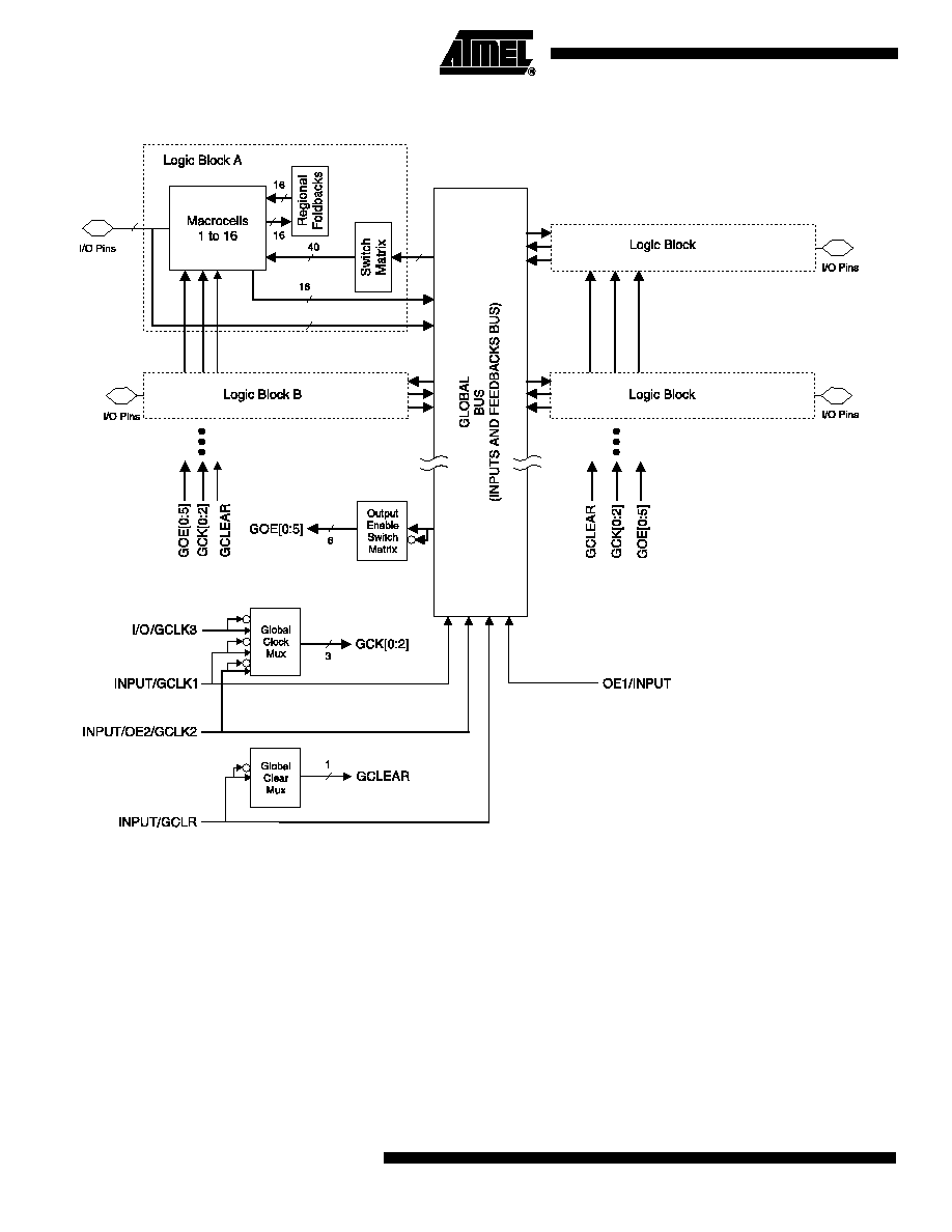
Global Bus/Switch
Matrix
The global bus (Figure 1) contains all input and I/O pin signals as well as the buried feedback
signals from all macrocells. The switch matrix in each logic block receives as its inputs all sig-
nals from the global bus. Up to 40 of these signals can be selected as inputs to the individual
logic blocks by the fitter software. Atmel's ATF15xx Family of CPLDs use a single level switch
matrix signal distribution structure, where each logic block input has access to the same num-
ber of global bus inputs, maximizing the number of possible ways to route a global bus signal.
This single level structure is in contrast with split switch matrix structures used by others in
which routing a particular global bus input to a particular logic block input makes that signal
unavailable to some other logic blocks, thus greatly limiting the available opportunities to
route.
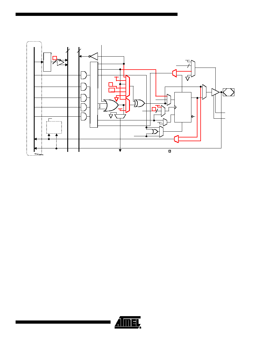
The ATF15xxSE Family macrocell, shown in Figure 2, consists of five sections: product terms
and product term select multiplexer, OR/XOR/CASCADE logic, foldback bus, a flip-flop and
output buffer. Extra fan-in and signal routing are provided throughout. Each macrocell can
generate a foldback logic term from the product term mux and a buried feedback with extra
routing that go to the global bus.
4
ATF15xxSE Family
2401D≠PLD≠09/02
Figure 1. ATF15xxSE Family Typical Block Diagram
6 to 16
N
N-1
6 to 16
5
ATF15xxSE Family
2401D≠PLD≠09/02
Figure 2. ATF15xxSE Family Macrocell with Enhanced Features In Red
Product Terms and
Select Mux
Within each macrocell are five product terms. Each product term may receive as its inputs any
combination of the signals from the switch matrix or regional foldback bus. The product term
select multiplexer (PTMUX) allocates the five product terms as needed to the macrocell logic
gates and control signals. The PTMUX programming is determined by the fitter software,
which selects the optimum macrocell configuration.
OR/XOR/
CASCADE Logic
Within a single macrocell, all the product terms can be routed to the OR gate, creating a 5-
input AND/OR sum term. With the addition of the CASIN from neighboring macrocells, this can
be expanded to as many as 40 product terms with little additional delay.
The macrocell's XOR gate allows efficient implementation of compare and arithmetic func-
tions. One input to the XOR comes from the OR sum term. The other XOR input can be a
product term or a fixed high- or low-level. For combinatorial outputs, the fixed level input
allows polarity selection. For registered functions, the fixed levels allow DeMorgan minimiza-
tion of product terms. The XOR gate may be fed from the flip-flop output to emulate T- and JK-
type flip-flops, or fed to the buried feedback to synthesize an extra latch.
Foldback Bus
Each macrocell can also generate a foldback product term. This signal goes to the regional
bus and is available to the 16 macrocells in a given logic block. The foldback is an inverse
polarity of one of the macrocell's product terms. Although Cascade Logic is the preferred
method for expanding the number of macrocell inputs to as many as 40, the 16 foldback terms
in each region can also generate additional fan-in sum terms with nominal additional delay.
REGIONAL
FOLDBACK
BUS
16
LOGIC
FOLDBACK
I/O Pin
3
GCK[0:2]
GCLEAR
CASOUT
D/
T*/L
CE
AR
AP
Q
CASIN
I/O Pin
SLEW
RATE
OPEN
COLLECTOR
6
GOE[0:5]
Reduced Power Option
S
W
I
T
C
H
M
A
T
R
I
X
80
GLOBAL BUS
40
1
2
3
4
5
P
r
o
d
u
c
t
T
e
r
m
M
U
X
PT1
PT2
PT3
PT5
PT4
SWITCH
MATRIX
OUTPUTS
* T flip-flop synthesised
!Q
Q
!Q
CK/CK
/LE
GOE
SWITCH
MATRIX
GOE [0:5]