1
Rev. 0403E≠06/98
High-
Performance
EE PLD
ATF16LV8C
Features
∑
3.0V to 5.5V Operation
∑
Industry Standard Architecture
≠ Emulates Many 20-Pin PALs
Æ
≠ Low Cost Easy-to-Use Software Tools
∑
High Speed
≠ 10 ns Maximum Pin-to-Pin Delay
∑
Ultra-Low Power
≠ 5
µ
µ
µ
µ
A (Max.) Pin-Controlled Power Down Mode Option
≠ Typical 100 nA Standby
∑
CMOS and TTL Compatible Inputs and Outputs
≠ I/O Pin Keeper Circuits
∑
Advanced Flash Technology
≠ Reprogrammable
≠ 100% Tested
∑
High Reliability CMOS Process
≠ 20 Year Data Retention
≠ 100 Erase/Write Cycles
≠ 2,000V ESD Protection
≠ 200 mA Latchup Immunity
∑
Commercial and Industrial Temperature Ranges
∑
Dual-in-Line and Surface Mount Packages in Standard Pinouts
Description
The ATF16LV8C is a high-performance EECMOS Programmable Logic Device that
utilizes Atmel's proven electrically erasable Flash memory technology. Speeds down
to 10 ns and a 5
µ
A pin-controlled power down mode option are offered. All speed
ranges are specified over the full 3.0V to 5.25V range for industrial and commercial
temperature ranges.
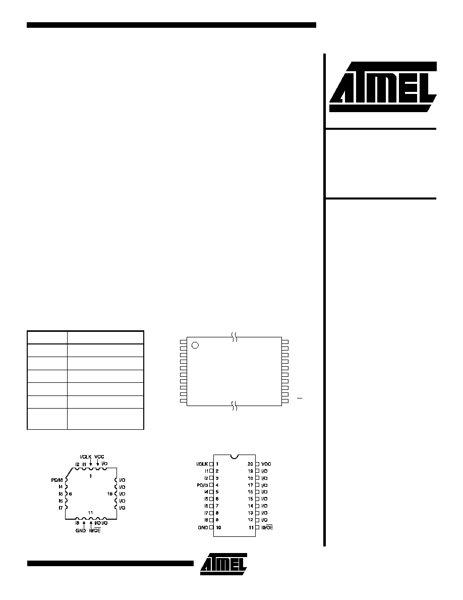
Pin Configurations
Pin Name
Function
CLK
Clock
I
Logic Inputs
I/O
Bidirectional Buffers
OE
Output Enable
VCC
(+3V to 5.5V) Supply
PD
Programmable Power
Down Option
PLCC
Top View
DIP/SOIC
TSSOP
1
2
3
4
5
6
7
8
9
10
20
19
18
17
16
15
14
13
12
11
I/CLK
I1
I2
PD/I3
I4
I5
I6
I7
I8
GND
VCC
I/O
I/O
I/O
I/O
I/O
I/O
I/O
I/O
19/OE
(continued)
ATF16LV8C
2
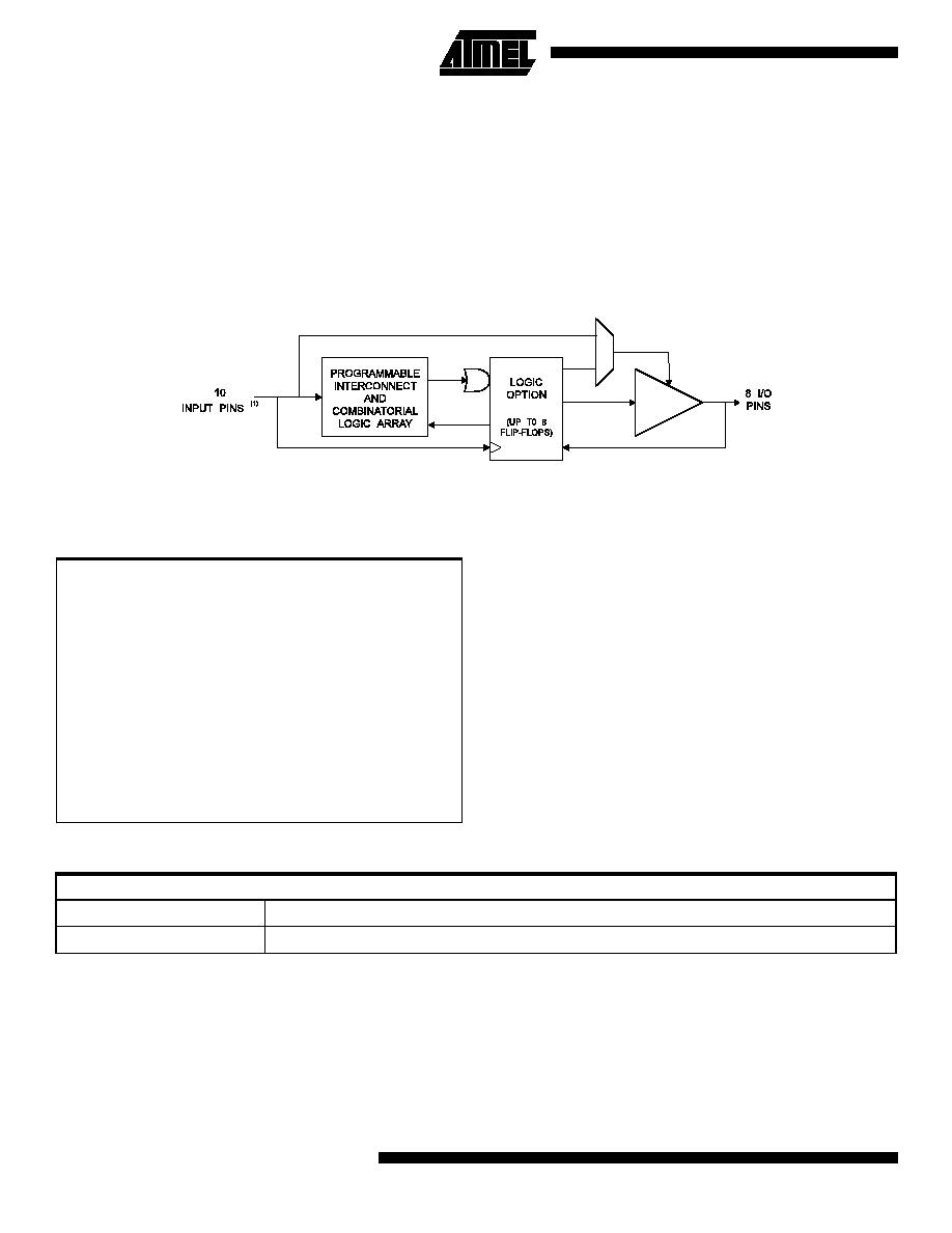
The ATF16LV8C incorporates a superset of the generic
architectures, which allows direct replacement of the 16R8
family and most 20-pin combinatorial PLDs. Eight outputs
are each allocated eight product terms. Three different
modes of operation, configured automatically with soft-
ware, allow highly complex logic functions to be realized.
The ATF16LV8C can significantly reduce total system
power, thereby enhancing system reliability and reducing
power supply costs. When pin 4 is configured as the power
down control pin, supply current drops to less than 5
µ
A
whenever the pin is high. If the power down feature isn't
required for a particular application, pin 4 may be used as a
logic input. Also, the pin keeper circuits eliminate the need
for internal pull-up resistors along with their attendant
power consumption.
Block Diagram
Note:
1.
Includes optional PD control pin.
Absolute Maximum Ratings*
Temperature Under Bias .................................. -40∞C to +85∞C
*NOTICE:
Stresses beyond those listed under "Absolute
Maximum Ratings" may cause permanent dam-
age to the device. This is a stress rating only and
functional operation of the device at these or any
other conditions beyond those indicated in the
operational sections of this specification is not
implied. Exposure to absolute maximum rating
conditions for extended periods may affect device
reliability.
Note:
1.
Minimum voltage is -0.6V dc, which may under-
shoot to -2.0V for pulses of less than 20 ns. Max-
imum output pin voltage is Vcc + 0.75V dc, which
may overshoot to 7.0V for pulses of less than 20
ns.
Storage Temperature ..................................... -65∞C to +150∞C
Voltage on Any Pin with
Respect to Ground .........................................-2.0V to +7.0V
(1)
Voltage on Input Pins
with Respect to Ground
During Programming.....................................-2.0V to +14.0V
(1)
Programming Voltage with
Respect to Ground .......................................-2.0V to +14.0V
(1)
DC and AC Operating Conditions
Commercial
Operating Temperature (Case)
0
∞
C - 70
∞
C
V
CC
Power Supply
3.0V to 5.5V
ATF16LV8C
3
Note:
1. All I
CC
parameters measured with outputs open.
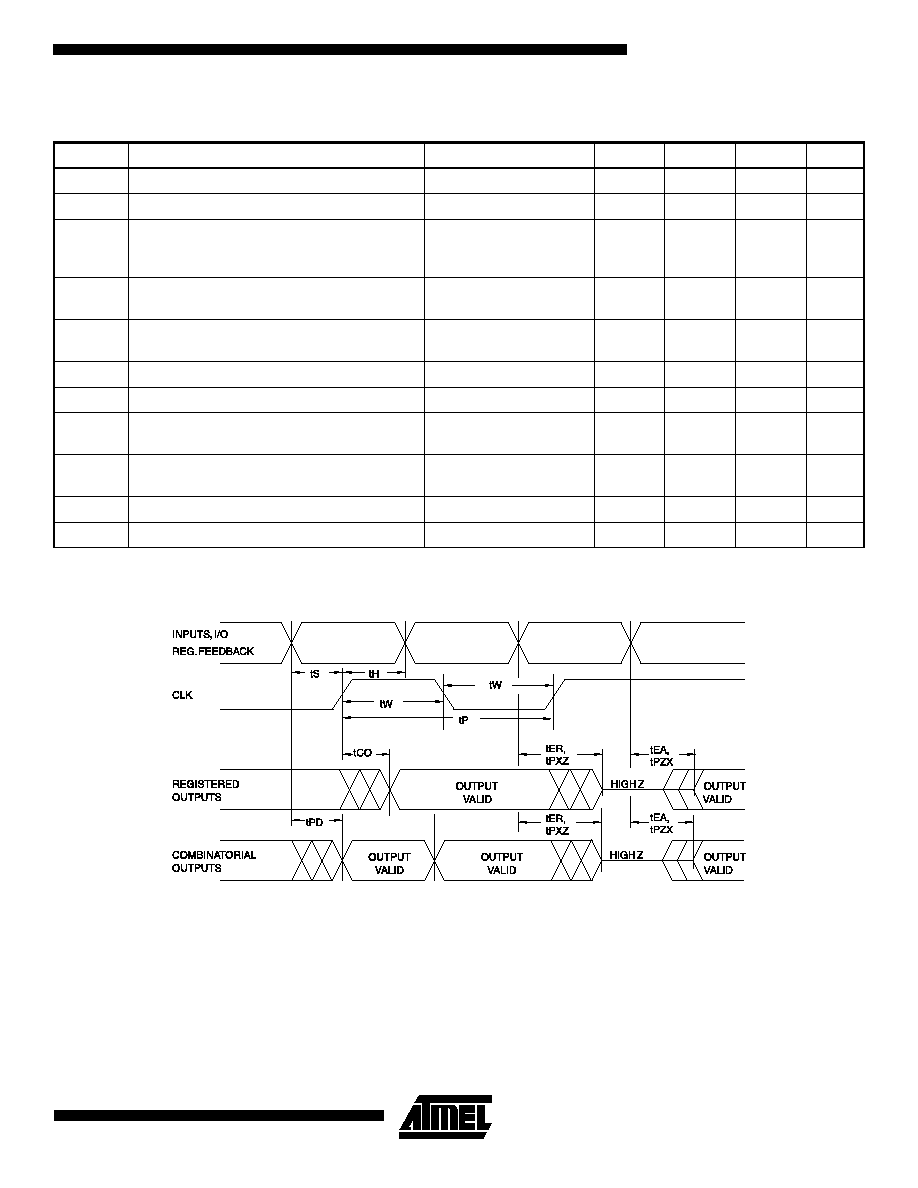
AC Waveforms
(1)
Note:
1.
Timing measurement reference is 1.5V. Input AC driving levels are 0.0V and 3.0V, unless otherwise specified.
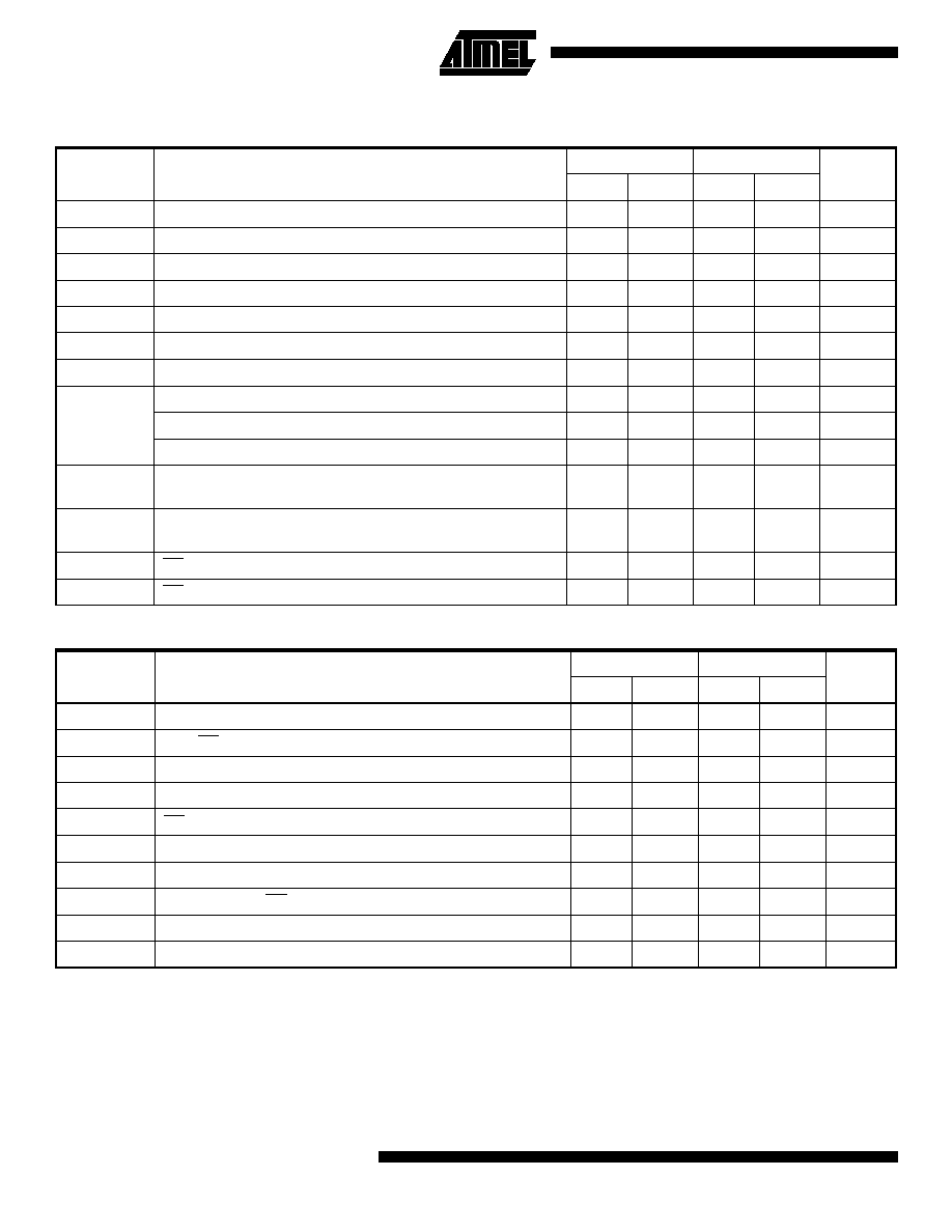
DC Characteristics
Symbol
Parameter
Condition
Min
Typ
Max
Units
I
IL
Input or I/O Low Leakage Current
0
V
IN
V
IL
(MAX)
-10
µ
A
I
IH
Input or I/O High Leakage Current
1.8
V
IN
V
CC
10
µ
A
I
CC1
(1)
Power Supply Current
15 MHz, V
CC
= MAX,
V
IN
= 0, V
CC,
Outputs Open
55
mA
I
PD
(1)
Power Supply Current, Power Down Mode
V
CC
= MAX,
V
IN
= 0, V
CC
0.1
5
µ
A
I
OS
Output Short Circuit Current
V
OUT
= 0.5V;
V
CC
= 3V; T
A
= 25∞C
-150
mA
V
IL
Input Low Voltage
MIN < V
CC
< MAX
-0.5
0.8
V
V
IH
Input High Voltage
2.0
V
CC
+ 1
V
V
OL
Output Low Voltage
V
CC
= MIN; All Outputs
I
OL
= 8 mA
0.5
V
V
OH
Output High Voltage
V
CC
= MIN
I
OL
= -500 mA
2.4
V
I
OL
Output Low Current
V
CC
= MIN
8
mA
I
OH
Output High Current
V
CC
= MIN
-4
mA
ATF16LV8C
4
Notes:
1. Output data is latched and held.
2. HI-Z outputs remain HI-Z.
3. Clock and input transitions are ignored.
AC Characteristics
Symbol
Parameter
-10
-15
Units
Min
Max
Min
Max
t
PD
Input or Feedback to Non-Registered Output
1
10
1
15
ns
t
CF
Clock to Feedback
5
8
ns
t
CO
Clock to Output
2
7
2
10
ns
t
S
Input or Feedback Setup Time
7
12
ns
t
H
Input Hold Time
0
0
ns
t
P
Clock Period
12
16
ns
t
W
Clock Width
6
8
ns
F
MAX
External Feedback 1/(t
S
+ t
CO
)
71.4
45.5
MHz
Internal Feedback 1/(t
S
+ t
CF
)
83.3
50
MHz
No Feedback 1/(t
P
)
83.3
62.5
MHz
t
EA
Input to Output Enable --
Product Term
3
10
3
15
ns
t
ER
Input to Output Disable --
Product Term
2
10
2
15
ns
t
PZX
OE pin to Output Enable
2
8
2
15
ns
t
PXZ
OE pin to Output Disable
1.5
8
1.5
15
ns
Power Down AC Characteristics
(1)(2)(3)
Symbol
Parameter
-10
-15
Units
Min
Max
Min
Max
t
IVDH
Valid Input Before PD High
10
15
ns
t
GVDH
Valid OE Before PD High
0
0
ns
t
CVDH
Valid Clock Before PD High
0
0
ns
t
DHIX
Input Don't Care After PD High
10
15
ns
t
DHGX
OE Don't Care After PD High
10
15
ns
t
DHCX
Clock Don't Care After PD High
10
15
ns
t
DLIV
PD Low to Valid Input
10
15
ns
t
DLGV
PD Low to Valid OE
25
30
ns
t
DLCV
PD Low to Valid Clock
25
30
ns
t
DLOV
PD Low to Valid Output
30
35
ns
ATF16LV8C
5
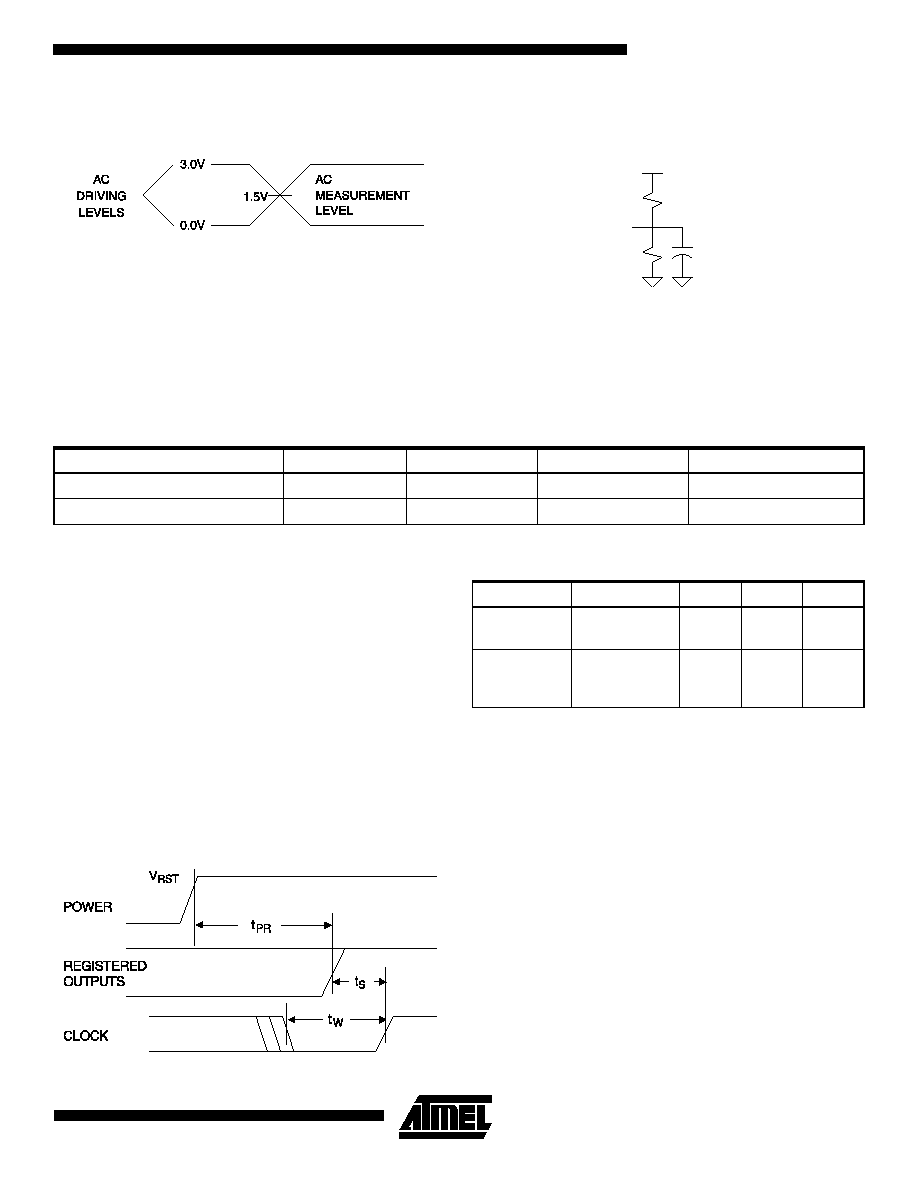
Input Test Waveforms and
Measurement Levels:
t
R
, t
F
< 1.5ns (10% to 90%)
Output Test Loads:
Commercial
Note:
Similar devices are tested with slightly different loads.
These load differences may affect output signals' delay
and slew rate. Atmel devices are tested with sufficient
margins to meet compatible devices.
Note:
1. Typical values for nominal supply voltage. This parameter is only sampled and is not 100% tested.
Power Up Reset
The ATF16LV8C's registers are designed to reset during
power up. At a point delayed slightly from V
CC
crossing
V
RST
, all registers will be reset to the low state. As a result,
the registered output state will always be high on power-up.
This feature is critical for state machine initialization. How-
ever, due to the asynchronous nature of reset and the
uncertainty of how V
CC
actually rises in the system, the fol-
lowing conditions are required:
1.
The V
CC
rise must be monotonic from below 0.7
volts.
2.
The signals from which the clock is derived must
remain stable during T
PR
.
3.
After T
PR
, all input and feedback setup times must
be met before driving the clock term high.
OUTPUT
PIN
3.3V
CL = 35 pF
R1 = 316
R2 = 348
Pin Capacitance
(f = 1 MHz, T = 25∞C)
(1)
Typ
Max
Units
Conditions
C
IN
5
8
pF
V
IN
= 0V
C
OUT
6
8
pF
V
OUT
= 0V
Parameter
Description
Typ
Max
Units
T
PR
Power-Up
Reset Time
600
1,000
ns
V
RST
Power-Up
Reset
Voltage
2.5
3.0
V