1
Features
∑
Next Generation Equivalent of ATF20V8B (ATF20V8BQ, ATF22V10BQC)
∑
Complimentary Easy-to-use Atmel-WinCUPL Design Software
∑
"Z" Zero Power Compared to "L" Low Power
∑
Edge-sensing Zero Standby Power (10 µA Typical) (CQZ)
∑
Pin-controlled Zero Standby Power (10 µA Typical) Option (C, CQ)
∑
User-controlled Power-down Pin (C, CQ)
∑
High-speed Electrically Erasable Programmable Logic Devices
≠ 5 ns Maximum Pin-to-pin Delay (C)
∑
CMOS and TTL Compatible Inputs and Outputs
≠ Pin-keeper Feature Holds Inputs and I/Os to Previous Logic States
≠ PCI Compliant
∑
High-reliability EE Process
≠ 20 Year Data Retention
≠ 100 Erase/Write Cycles
≠ 2,000V ESD Protection
≠ 200 mA Latch-up Immunity
∑
Commercial and Industrial Temperature Ranges
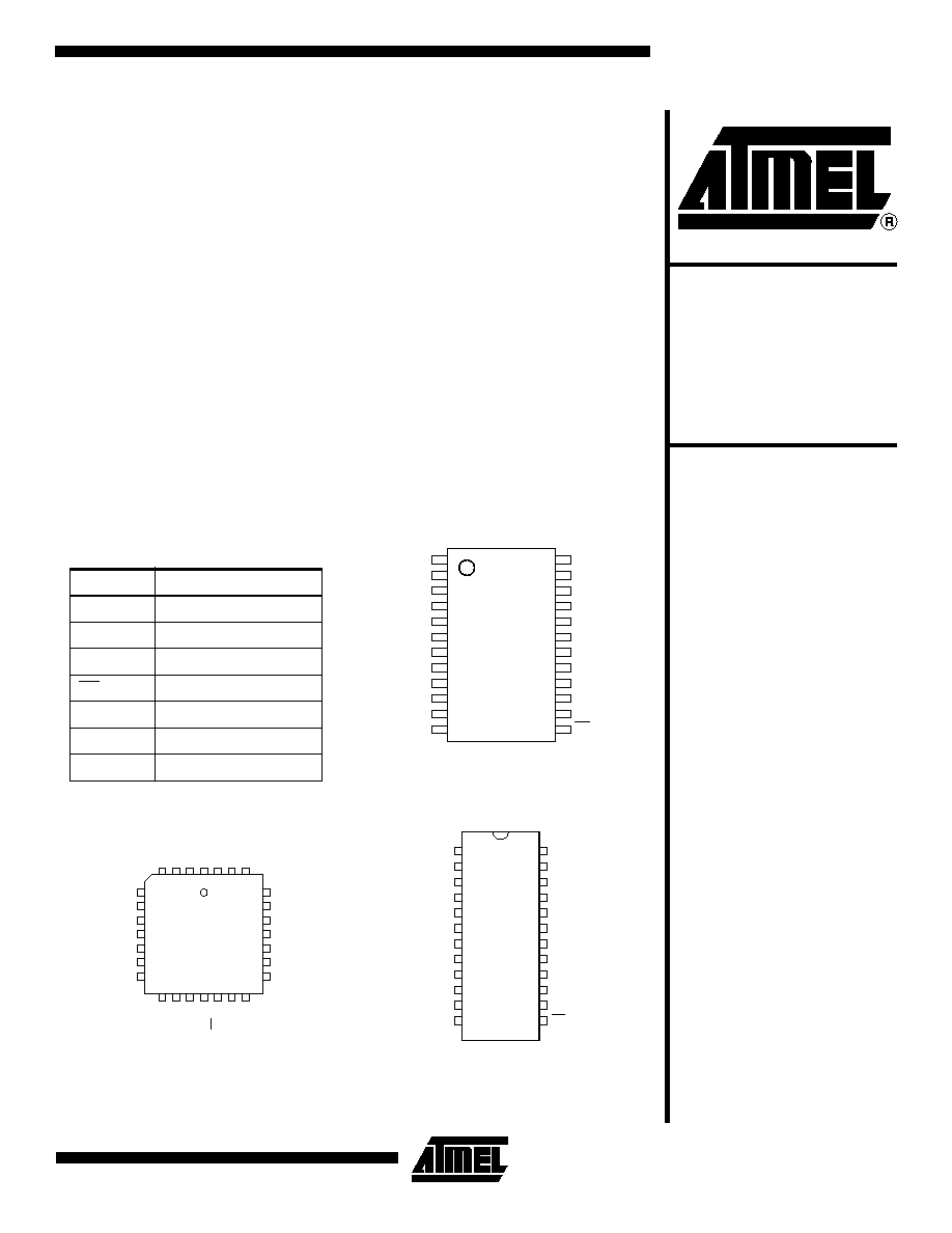
AT20V8C Family
High-
performance
EE PLD
ATF20V8C
ATF20V8CQ
ATF20V8CQZ
Rev. 0408H≠04/01
Pin Configurations
All Pinouts Top View
Pin Name
Function
CLK
Clock
IN
Logic Inputs
I/O
Bi-directional Buffers
OE
Output Enable
NC
No Internal Connection
VCC
+5V Supply
PD
Power-down
TSSOP
1
2
3
4
5
6
7
8
9
10
11
12
24
23
22
21
20
19
18
17
16
15
14
13
CLK/IN
IN
IN
IN
IN
IN
IN
IN
IN
IN
IN
GND
VCC
IN
I/O
I/O
I/O
I/O
I/O
I/O
I/O
I/O
IN
OE/IN
(1)
PD/
PLCC
5
6
7
8
9
10
11
25
24
23
22
21
20
19
(1)
PD/IN
IN
IN
NC
IN
IN
IN
I/O
I/O
I/O
NC
I/O
I/O
I/O
4
3
2
1
28
27
26
12
13
14
15
16
17
18
IN
IN
GND
NC
OE/IN
IN
I/O
IN
IN
CLK/IN
NC
VCC
IN
I/O
DIP/SOIC
1
2
3
4
5
6
7
8
9
10
11
12
24
23
22
21
20
19
18
17
16
15
14
13
CLK/IN
IN
IN
(1)
PD/IN
IN
IN
IN
IN
IN
IN
IN
GND
VCC
IN
I/O
I/O
I/O
I/O
I/O
I/O
I/O
I/O
IN
OE/IN
Note:
1. PD on C and CQ only.
2
ATF20V8C Family
0408H≠04/01
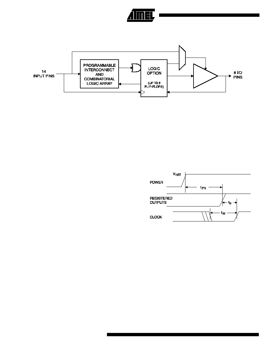
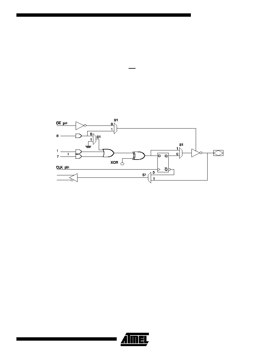
Block Diagram
Description
The ATF20V8C is a high-performance CMOS (electrically
erasable) programmable logic device (PLD) that utilizes
Atmel's proven electrically erasable technology. Speeds
down to 5 ns and power dissipation as low as 10 µA are
offered. All speed ranges are specified over the full 5V ±
10% range for industrial temperature ranges, and 5V ± 5%
for commercial ranges.
The ATF20V8C(Q) provides a high-speed CMOS PLD
solution with maximum pin-to-pin delay of 5 ns. The
ATF20V8C(Q) also has a user-controlled power-down fea-
ture, offering "zero" standby power (10 µA typical). The
user-controlled power-down feature allows the user to
manage total system power to meet specific application
requirements and enhance reliability without sacrificing
speed.
The ATF20V8CQZ provides the zero power CMOS PLD
solution, with "zero" standby power (10 µA typical). The
device powers down automatically through Atmel's pat-
ented Input Transition Detection (ITD) circuitry to the "zero"
standby power mode when all inputs are idle.
Pin "keeper" circuits on input and output pins reduce static
power consumed by pull-ups.
The ATF20V8C(Q)(Z) is the industry-standard 20V8 archi-
tecture. Eight outputs are each allocated eight product
terms. Three different modes of operation, configured auto-
matically with software, allow highly complex logic
functions to be realized.
Power-up Reset
The registers in the ATF20V8Cs are designed to reset dur-
ing power-up. At a point delayed slightly from V
CC
crossing
V
RST
, all registers will be reset to the low state. As a result,
the registered output state will always be high on power-up.
This feature is critical for state machine initialization. How-
ever, due to the asynchronous nature of reset and the
uncertainty of how V
CC
actually rises in the system, the fol-
lowing conditions are required:
1.
The V
CC
rise must be monotonic,
2.
After reset occurs, all input and feedback setup
times must be met before driving the clock pin high,
and
3.
The clock must remain stable during t
PR
.
Preload of Registered Outputs
The ATF20V8C registers are provided with circuitry to
allow loading of each register with either a high or a low.
This feature will simplify testing since any state can be
forced into the registers to control test sequencing. A
JEDEC file with preload is generated when a source file
with vectors is compiled. Once downloaded, the JEDEC file
preload sequence will be done automatically by most of the
approved programmers after the programming.
Electronic Signature Word
There are 64 bits of programmable memory that are always
available to the user, even if the device is secured. These
bits can be used for user-specific data.
3
ATF20V8C Family
0408H≠04/01
Security Fuse Usage
A single fuse is provided to prevent unauthorized copying
of the ATF20V8C's fuse patterns. Once programmed, fuse
verify and preload are inhibited. However, the 64-bit User
Signature remains accessible.
The security fuse should be programmed last, as its effect
is immediate.
Programming/Erasing
Programming/erasing is performed using standard PLD
programmers. For further information, see the Configurable
Logic data book section titled, "CMOS PLD Programming
Hardware and Software Support."
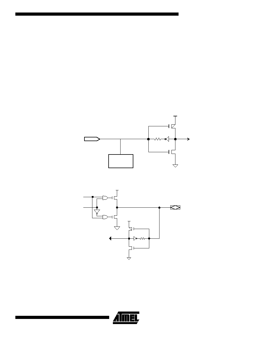
Input and I/O Pull-ups
All ATF20V8C family members have internal input and I/O
"pin-keeper" circuits. Therefore, whenever inputs or I/Os
are not being driven externally, they will maintain their last
driven state. This ensures that all logic array inputs and
device outputs are at known states. These are relatively
weak active circuits that can be easily overridden by TTL-
compatible drivers (see input and I/O diagrams below).
Input Diagram
I/O Diagram
100K
V
CC
ESD
PROTECTION
CIRCUIT
INPUT
100K
VCC
VCC
DATA
OE
I/O
INPUT
4
ATF20V8C Family
0408H≠04/01
Functional Logic Diagram Description
The logic option and functional diagrams describe the
ATF20V8C architecture. Eight configurable macrocells can
be configured as a registered output, combinatorial I/O,
combinatorial output or dedicated input.
The ATF20V8C's macrocell can be configured in one of
three different modes. Each mode makes the ATF20V8Cs
look like a different device. The ATF20V8Cs can be a reg-
istered output, combinatorial I/O, combinatorial output or
dedicated input. Most PLD compilers can choose the right
mode automatically. The user can also force the selection
by supplying the compiler with a mode selection. The deter-
mining factors would be the usage of register versus
combinatorial outputs and dedicated outputs versus output
with output enable control.
The ATF20V8Cs have a user-controlled power-down pin,
which, when active, allows the user to place the device into
a "zero" standby power-down mode. The device can also
operate at high speed. Maximum pin-to-pin delays of 5 ns
are offered. Static power loss due to pull-up resistors is
eliminated by using input and output pin "keeper" circuits
that hold pins to their previous logic levels when idle.
The universal architecture of the ATF20V8Cs can be pro-
grammed to emulate many 24-pin PAL devices. The user
can download the subset device JEDEC programming file
to the PLD programmer and the ATF20V8Cs can be config-
ured to act like the chosen device.
Unused product terms are automatically disabled by the
compiler to decrease power consumption. A security fuse,
when programmed, protects the contents the ATF20V8Cs.
Eight bytes (64 fuses) of User Signature are accessible to
the user for purposes such as storing project name, part
number, revision or date. The User Signature is accessible
regardless of the state of the security fuse.
Note:
1. Only applicable for version 3.4 or lower.
Compiler Mode Selection
Registered
Complex
Simple
Auto Select
ABEL, Atmel-ABEL
P20V8R
P20V8C
P20V8
P20V8
CUPL
G20V8MS
G20V8MA
G20V8
G20V8A
LOG/iC
GAL20V8_R
(1)
GAL20V8_C7
(1)
GAL20V8_C8
(1)
GAL20V8
OrCAD-PLD
"Registered"
"Complex"
"Simple"
GAL20V8
PLDesigner
P20V8
P20V8
P20V8
P20V8
Tango-PLD
G20V8
G20V8
G20V8
G20V8
5
ATF20V8C Family
0408H≠04/01
Registered Mode
PAL Device Emulation/PAL Replacement
The registered mode is used if one or more registers are
required. Each macrocell can be configured as either a reg-
istered or combinatorial output or I/O, or as an input. For a
registered output or I/O, the output is enabled by the OE
pin, and the register is clocked by the CLK pin. Eight prod-
uct terms are allocated to the sum term. For a combinato-
rial output or I/O, the output enable is controlled by a
product term, and seven product terms are allocated to the
sum term. When the macrocell is configured as an input,
the output enable is permanently disabled.
Any register usage will make the compiler select this mode.
The following registered devices can be emulated using
this mode:
20R8
20RP8
20R6
20RP6
20R4
20RP4
Registered Mode Operation