1
5319A≠IMAGE≠04/03
Main Features
∑
High Sensitivity Full Frame CCD Sensor
∑
2300 x 3500 Resolution with 10 µm Square Pixels
∑
100% Aperture Pixels
∑
12-bit Dynamic Range
∑
Very Low Noise: 65 dB SNR
∑
Binning and ROI Modes
∑
LVDS or CameraLink Data Format (Base Configuration)
∑
High Data Rate: 25 Mpixels/s
∑
Flexible and Easy to Operate via RS-232 Control
≠ Trigger Mode: Free Run or External Trigger Modes
≠ Binning 2 x 2 and 4 x 4, Up to 5 ROI
≠ Exposure Time
≠ Gain: -5 to 29 dB by Step of 0.04 dB
≠ Offset: 0 to 255 LSB
≠ 3-Shot Color Operation
≠ Test Pattern Generation
∑
Single Power Supply: 24V
DC
∑
High Reliability ≠ CE and FCC Compliant
∑
F (Nikon) Mount Adapter (Lens Not Supplied)
Product Description
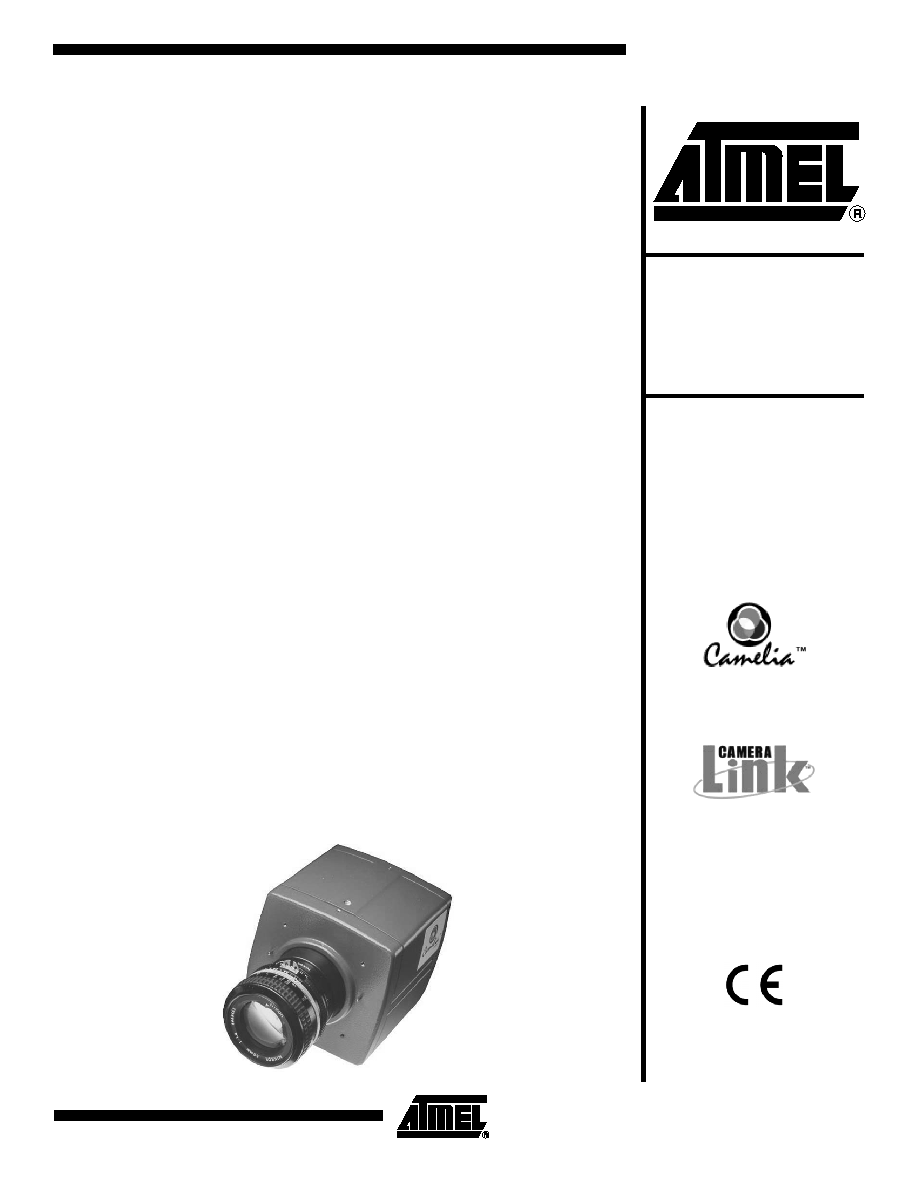
This camera is designed to meet high performance and quality requirements while
providing ease of use.
∑
Atmel manages the entire process, from the sensor to the camera. The result is a
camera able to work in 12 bits, with dedicated electronics that provide excellent
signal to noise ratio.
∑
Because of the 100% aperture pixel the sensitivity of the camera is fairly high
even in near infrared.
∑
The programmable settings let the user work with different integration times, gains
and offsets. The external trigger allows the user to synchronize the camera on an
external event while the 3-shot color mode allows very high resolution for color
image acquisition.
Applications
The performance and reliability of this camera make it well suited for the most
demanding applications such as film and document scanning, semiconductor and
PCB inspection, DNA analysis, metrology, X-ray imaging, etc...
B & W 8 Megapixels
LVDS and
CameraLink
TM
Digital Cameras
CAMELIA M1 LV 8M
CAMELIA M1 CL 8M
Preliminary
Rev. 5319A≠IMAGE≠04/03

2
CAMELIA M1 8M LVDS and CameraLink Camera
5319A≠IMAGE≠04/03
Improvements
The Camelia 8M has been redesigned:
∑
To add new features:
≠
Gain: 928 steps from -5 to 29 dB
≠
Offset: 0 to 255 LSB
≠
Test pattern: ramps up from 0 to 2298 pixel values on each line
≠
Median filter: to remove 1 x 1 and columns defects
∑
To improve the electro-optical performances, in particular by:
≠
Reducing power consumption from 8.5W down to 5.5W, using a new front
panel and internal heat sink. This lowers the CCD temperature by 5
∞
C thus
decreasing the magnitude of "white pixels".
≠
Decreasing the typical temporal noise from 2.7 to 2.4 LSB
∑
To interface with more standard and more cost effective cables
∑
To improve reliability
∑
Camelia M1 8M is CE and FCC compliant
What changes for the user?
∑
New additional commands for gain, offset and test pattern
∑
RS-232 transmission speed increased from 9600 to 19200 bauds for LVDS
cameras (9600 bauds for CameraLink cameras)
∑
Interface connectors:
≠
DATA & SYNC is a 3M MDR connector with better availability, the same
pinout but different mechanic
≠
RS-232 is a D-Sub 9 female for full-duplex transmission
≠
The power supply connector has a camera standard pinout
≠
TTL CONTROL is a new D-Sub 9 male connector avoiding the use of a Y
cable
∑
New rear panel (see position of connectors)

3
CAMELIA M1 8M LVDS and CameraLink Camera
5319A≠IMAGE≠04/03
Imaging System
Description
Figure 1. LVDS Camera Imaging System
Figure 2. CameraLink Camera Imaging System

4
CAMELIA M1 8M LVDS and CameraLink Camera
5319A≠IMAGE≠04/03
The Camelia camera is powered by a single +24V power supply. It is configurable via
the serial port of the computer (by using either CommCam software or standard RS-232
communicator as TTY or Hyperterminal) for LSD cameras. Camelia is configurable via
the serial communication of CameraLink for CameraLink cameras. It also sends digital
video.
As Camelia's CCD is a full frame sensor, the user must use either pulsed lighting or a
chopper/shutter in front of the camera in order to have only incident lighting on the CCD
during integration time. The user must design an electro-optical interface to drive the
camera, the shutter/chopper or lighting by using the SHUTTER signal delivered by the
camera. If required, the system can send an external trigger or external ITC (integration
time control signal) to the camera.
The BG38 Filter is essential to have a correct white balance on Color Cameras and for
use with standard optics (for achromaticity purpose).
Note that the following Elements are not provided by Atmel:
∑
Shutter (LCD or Mechanical)
∑
BG38 (Anti-infra Red) Filter
∑
Control Box
∑
Lens
∑
Light Source
∑
+24V Power Supply
∑
Computer
For a complete explanation of the utility of the BG38 Filter and the Shutter, please con-
sult the associated FAQ and the sample images on the Atmel's "Camera Documentation
& Software" CD-Rom.

5
CAMELIA M1 8M LVDS and CameraLink Camera
5319A≠IMAGE≠04/03
CCD Description
Image Format
35.0 mm (V) x 23.0 mm (H)
Figure 3. Sensor Organization
Note:
The camera does not output to the 16 dark references.
Active Pixels
Readout Register
The readout register is along the small side of the image area (vertical image).
Pixel Geometry
Pixels are 10 µm x 10 µm with an aperture ratio of 100%.
Antiblooming by
Clocking
Antiblooming can be activated or inhibited (see "Serial Communication" on page 12):
∑
Antiblooming OFF: antiblooming inhibited. This position is recommended if
antiblooming is not required for the application.
∑
Antiblooming ON: antiblooming activated.
∑
When binning is disabled, the antiblooming is typically efficient up to 8 times
saturation light.
MPP Photosensitive Zone
Output Register
16 Dark References
3500 Lines
2300 Columns
- 100% aperture
- 10
µ
m square pixels
Table 1. Active Pixels
Mode (set via serial com)
Image Size (H x V)
Timing Diagram Correspondence
No binning
2300 x 3500
H = M
V = N
2 x 2 pixel binning
1150 x 1750
4 x 4 pixel binning
574 x 875


