1
4728A≠CLOCK≠06/03
Features
∑
32-kHz Oscillator
∑
1.3 V to 1.8 V Operating-voltage Range
∑
180 nA Typical Current Consumption
∑
Voltage Regulator
∑
Integrated Capacitors, Mask Selectable
∑
Mask Options for Pad Designation, Motor Period and Motor Pulse Width
∑
Low Resistance Outputs for Bipolar Stepping Motor
∑
Motor Fast-test Function
Description
The e1217X is an integrated circuit in CMOS silicon gate technology for analog
watches. It consists of a 32-kHz oscillator, frequency dividers down to 1/64 Hz, output
pulse formers and push-pull motor drivers. Integrated capacitors are provided (select-
able mask option) for tuning of the crystal. Low current consumption and high
oscillator stability are enabled by an on-chip voltage regulator.
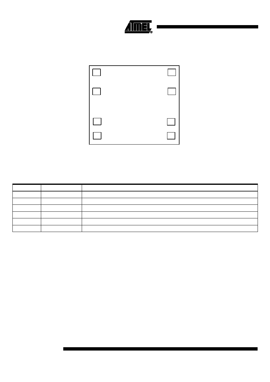
32-kHz
Standard Watch
CMOS IC
e1217X
3
e1217X
4728A≠CLOCK≠06/03
Functional Description
Voltage Regulator
An integrated voltage regulator provides the oscillator with a well-controlled negative
supply voltage V
REG
. This improves the stability of the oscillator and keeps current con-
sumption at a minimum.
Oscillator
The oscillator inverter with feedback resistor generates the 32768 Hz clock frequency. A
total capacitance of 24 pF is integrated. This can be selected for COSCOUT in 2 pF
increments via a mask option.
Frequency Divider
A 21-bit binary counter is provided, dividing the oscillator frequency down to 1/64 Hz.
The leading six stages are connected to V
DD
and V
REG
, while the remaining 15 stages
are connected to V
DD
and V
SS
.
Motor Drive Output
The e1217X contains two push-pull output buffers for driving bipolar stepping motors.
During a motor pulse, the n-channel device of one buffer and the p-channel device of
the other buffer are activated. The p-channel devices of both buffers are active (see Fig-
ure 3) between the two pulses.
Cycle time and pulse width can be chosen via a metal mask option (Table 1).
RESET
A debounced RESET input is provided. Connecting the RESET input to V
DD
resets the
12 low-order stages of the frequency divider, thus disabling further motor pulses. Motor
pulses, which are in progress when the reset function is applied, will be completed. After
releasing the RESET pad from V
DD
, the next motor pulse appears with a delay of one
half motor cycle on the drive output opposed to the former (Figure 4). Due to the
debounce circuitry on the RESET input, V
DD
must be applied for at least 31.2 ms. Dur-
ing RESET the input current is limited to 8 nA typically.
Test
A test frequency of 512 Hz is output to this pad which can be measured with a high
resistance probe (R
≥
10 M
W
, C
≥
20 pF). This signal can be used for testing and tuning
the oscillator. Connecting TEST to V
DD
for at least 4 ms changes the motor cycle time
from the selected value to the test cycle time (mask options), while the motor pulse
width remains unchanged (Figure 3).
This feature can be used to reduce the amount of time required for testing the mechani-
cal parts of the watch.
Table 1. Motor Options
Motor-cycle Parameters
Value
Cycle time T
M
2, 4, 6, 8, 10, 12, 20, 24, 30, 40, 60, 80, 120 s
Motor pulse width t
M
0.98 to 14.65 ms in increments of 0.98 ms
Motor test cycle time T
MT
250, 125, 62.5 ms
4
e1217X
4728A≠CLOCK≠06/03
Absolute Maximum Ratings
Absolute maximum ratings define parameter limits which, if exceeded, may permanently change or damage the device.
All inputs and outputs on Atmel's circuits are protected against electrostatic discharges. However, precautions to minimize
the build-up of electrostatic charges during handling are recommended.
The circuit is protected against supply-voltage reversal for typically 5 minutes.
Parameters
Symbol
Value
Unit
Supply voltage
V
SS
-0.3 to +5
V
Input voltage range, all inputs
V
IN
(V
SS
- 0.3
V)
£
V
IN
£
(V
DD
+ 0.3 V)
V
Output short-circuit duration
indefinite
Power dissipation (DIL package)
P
tot
125
mW
Operating ambient temperature range
T
amb
-20 to +70
∞
C
Storage temperature range
T
stg
-40 to +125
∞
C
Lead temperature during soldering at 2 mm
distance, 10 s
T
sld
260
∞
C
Operating Characteristics
V
DD
= 0 V; V
SS
= -1.55 V; T
amb
= +25
∞
C; C
TR
= 15 pF, unless otherwise specified.
All voltage levels are measured with reference to V
DD
. Test crystal as specified below.
Parameters
Test Conditions
Symbol
Min.
Typ.
(1)
Max.
Unit
Operating voltage
Functional test (Figure 2)
V
SS
-1.3
-1.8
V
Operating current
C
oscout
= 16 pF, R
L
= R
I
SS
-180
-300
nA
RESET input current
RESET = V
DD
I
R
8
nA
Motor Outputs
Motor output current
R
L
= 2 k
W
, V
SS
= -1.55 V
I
M
±0.7
mA
Motor period
T
M
See Table 2
s
Motor pulse width
T
M
See Table 2
ms
Motor test period
T
MT
See Table 2
ms
Oscillator
Stability
D
V
SS
= 100 mV, C
TR
= 5 pF
D
f/f
0.1
ppm
Start-up voltage
Startup within 2 s
V
ST
-1.3
V
Integrated input capacitor
C
OSC IN
See Table 2
pF
Integrated output capacitor
C
OSCOUTmax
= 24 pF
C
OSC OUT
See Table 2
pF
Note:
1. Typical parameters represent the statistical mean values.

5
e1217X
4728A≠CLOCK≠06/03
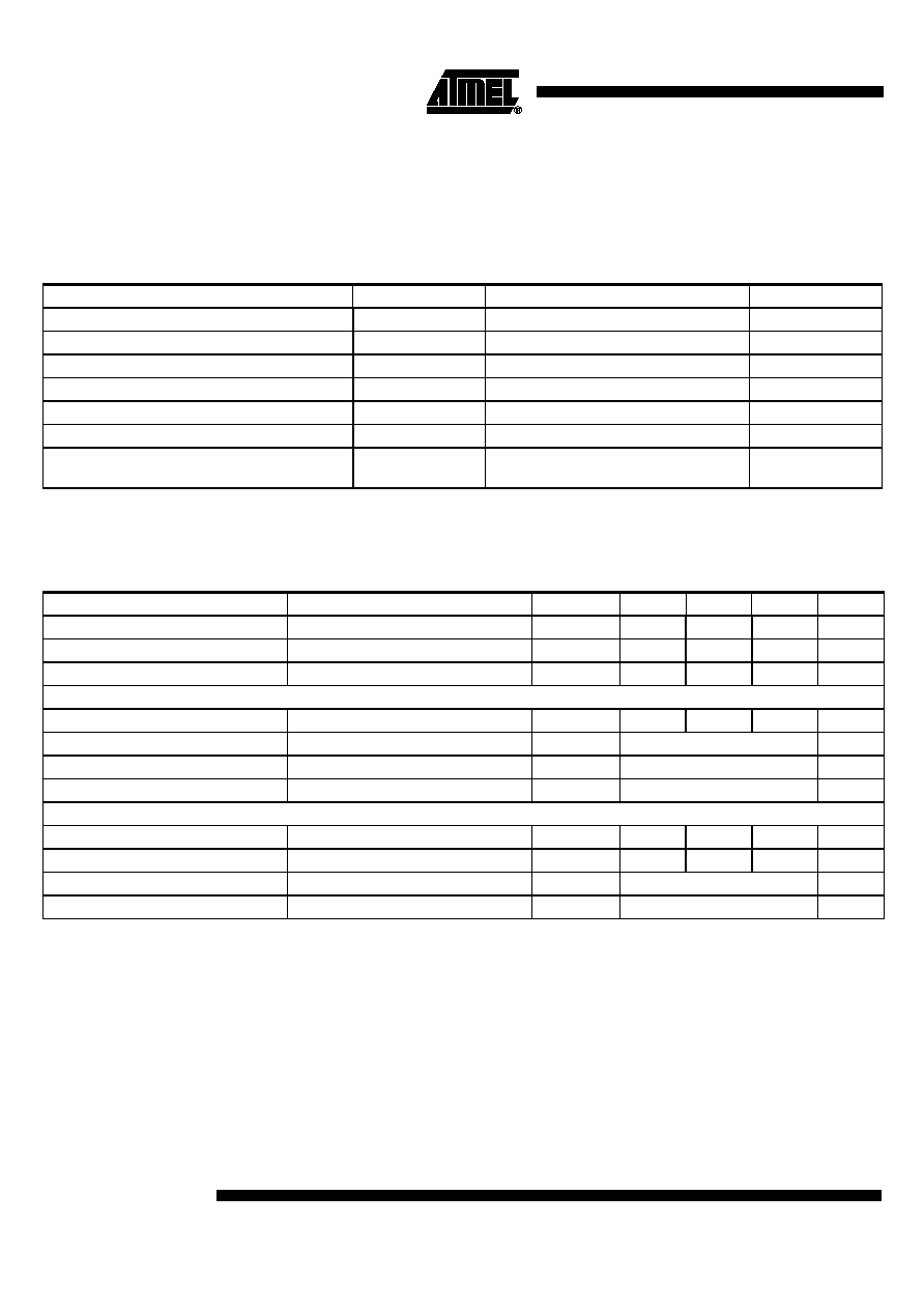
Figure 2. Functional Test Circuit
Range of trimmer capacitance: C
TR
= 5 pF to 30 pF
Test Crystal
Specification
Additional Notes
1.
It is recommended to connect the quartz case to V
DD
(by conductive epoxy).
2.
Capacitive coupling of TEST to OSCIN must be minimized by appropriate layout
of the PCB to avoid disturbancing the oscillator.
TEST
OSCIN
OSCOUT
MOT2
MOT1
RESET
e1217X
V
SS
C
TR
R
L
1
2
3
4
8
7
6
5
V
DD
Frequency
f = 32,768 Hz
Series resistance
R
S
= 30 k
W
Static capacitance
C
0
= 1.5 pF
Dynamic capacitance
C
1
= 3 fF
Load capacitance
C
L
= 8 pF