 | –≠–ª–µ–∫—Ç—Ä–æ–Ω–Ω—ã–π –∫–æ–º–ø–æ–Ω–µ–Ω—Ç: E5130A | –°–∫–∞—á–∞—Ç—å:  PDF PDF  ZIP ZIP |
e5130
Rev. A2, 13-Mar-01
1 (4)
Low Voltage CMOS Driver Circuit
Description
The e5130 contains 4 independent driver outputs with an
ON resistance of typ. 25
W (15 W) tor the P-channel
output transistors and typ. 20
W (13 W) for the N-channel
output transistors; at a supply voltage of 1.5 V (3 V). To
obtain a fast transition of the outputs, even for slow
rise/-fall time input signals, all digital inputs (IN1 ... IN4)
have a schmitt-trigger characteristic; with a hysteresis of
typ. 50 mV. If a higher driving capability is needed, all
inputs and outputs may be connected in parallel. In this
case the rise/-fall time of the input signals IN1 ... IN4 must
be less than 200 nsec. Due to the fast switching
characteristic of the tristatable output drivers, the circuit
is also suited as low voltage bus driver.
Features
D 1.1 ≠ 3.6 V operating voltage range
D 4 non-inverting, tristatable drivers for the
following applications:
≠
Motor driver for bipolar stepper motors in watch/-
clock applications
≠
Driver for piezoelectric transducers (buzzer)
≠
LED Driver
≠
Line driver for medium speed applications
Advantages
D High load current at low supply voltage
D Replaces several discrete transistors
D Tri-state operation possible
D Possible applications:
≠
Motor driver
≠
Radio controlled clock/watch
≠
Line driver for mini-computer, laptop
≠
LED driver
≠
Relay driver
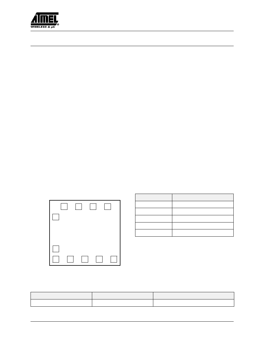
Pad Configuration
TRI
OUT2
OUT4
OUT3
OUT1
IN3
IN2
IN1
IN4
V
DD
V
SS
e5130
94 8178
Name
Description
V
DD
Positive supply voltage
V
SS
Negative supply voltage
IN1 ... IN4
Digital inputs
TRI
Tristate input
OUT1 ... OUT4
Drive outputs
Chipsize: x = 1.08 mm
, y = 1.42 mm,
Padwindow: 90 x 90
m
Ordering Information
Extended Type Number
Package
Remarks
e5130A≠DIT
Die
Die in Trays
e5130
Rev. A2, 13-Mar-01
2 (4)
Absolute Maximum Ratings
Absolute maximum ratings define parameter limits which, it exceeded, may permanently change or damage the device.
All inputs and outputs on circuits are highly protected against electrostatic discharges.
However, precautions to minimize build-up of electrostatic charges during handling are recommended.
The circuits are protected against supply voltage reversal for typically 5 minutes, if the current is limited to 120 mA.
Parameters
Symbol
Value
Unit
Supply voltage
V
DD
≠ V
SS
≠ 0.3 to + 5
V
Input voltage range, all inputs
V
I
V
SS
≠ 0.3 to V
DD
+ 0.3
V
Operating ambient temperature range
≠ 20 to + 70
∞
C
Storage temperature range
≠ 40 to + 125
∞
C
Lead temperature during soldering at 2 mm distance, 10 s
260
∞
C
Operating Characteristics
V
SS
= 0 V, V
DD
= + 1.5 V, T
amb
= + 25
∞
C, unless otherwise specified.
All voltage levels are measured with reference to V
SS
.
Parameters
Test Conditions / Pin
Symbol
Min
Typ
Max
Unit
Operating voltage
V
DD
1.1
3.6
V
Operating temperature
T
amb
≠ 10
60
∞
C
Operating current (standby)
V
DD
= 3.6 V, R
L12
= R
L34
=
R,
IN1 to IN4 at V
DD
or V
SS
, TRI at
V
SS
I
DD
0.05
1
mA
Drive output OUT1 to OUT4
Output current
V
DD
= 1.2 V, R
L12
= R
L34
= 200
W
I
OUT
" 4.3 " 4.75
mA
Output current
V
DD
= 1.5 V, R
L12
= R
L34
= 200
W
I
OUT
" 5.7 " 6.20
mA
Output current
V
DD
= 3.0 V, R
L12
= R
L34
= 200
W
I
OUT
" 12
" 13
mA
Delay time
V
DD
= 3 V, C
L
= 50 pF
T
Dr
, T
Df
35
60
ns
Delay time
V
DD
= 1.5 V, C
L
= 50 pF,
see figure 2, note 1
T
Dr
, T
Df
80
150
ns
Rise/-fall time
V
DD
= 3 V, C
L
= 50 pF
t
r
, t
f
8
15
ns
Rise/-fall time
V
DD
= 1.5 V, C
L
= 50 pF,
see figure 2, note 2
t
r
, t
f
12
25
ns
Digital input IN1 to IN4
Input current
V
IL
= 0 V
I
IL
≠100
nA
Input current
V
IH
= V
DD
I
IH
100
nA
Threshold
V
V
TH
V
DD
/2
V
Hysteresis
mV
V
HYST
50
mV
Tristate input TRI
Input current TRI
V
IH
= V
DD
I
IH
0.15
0.4
1.2
mA
e5130
Rev. A2, 13-Mar-01
3 (4)
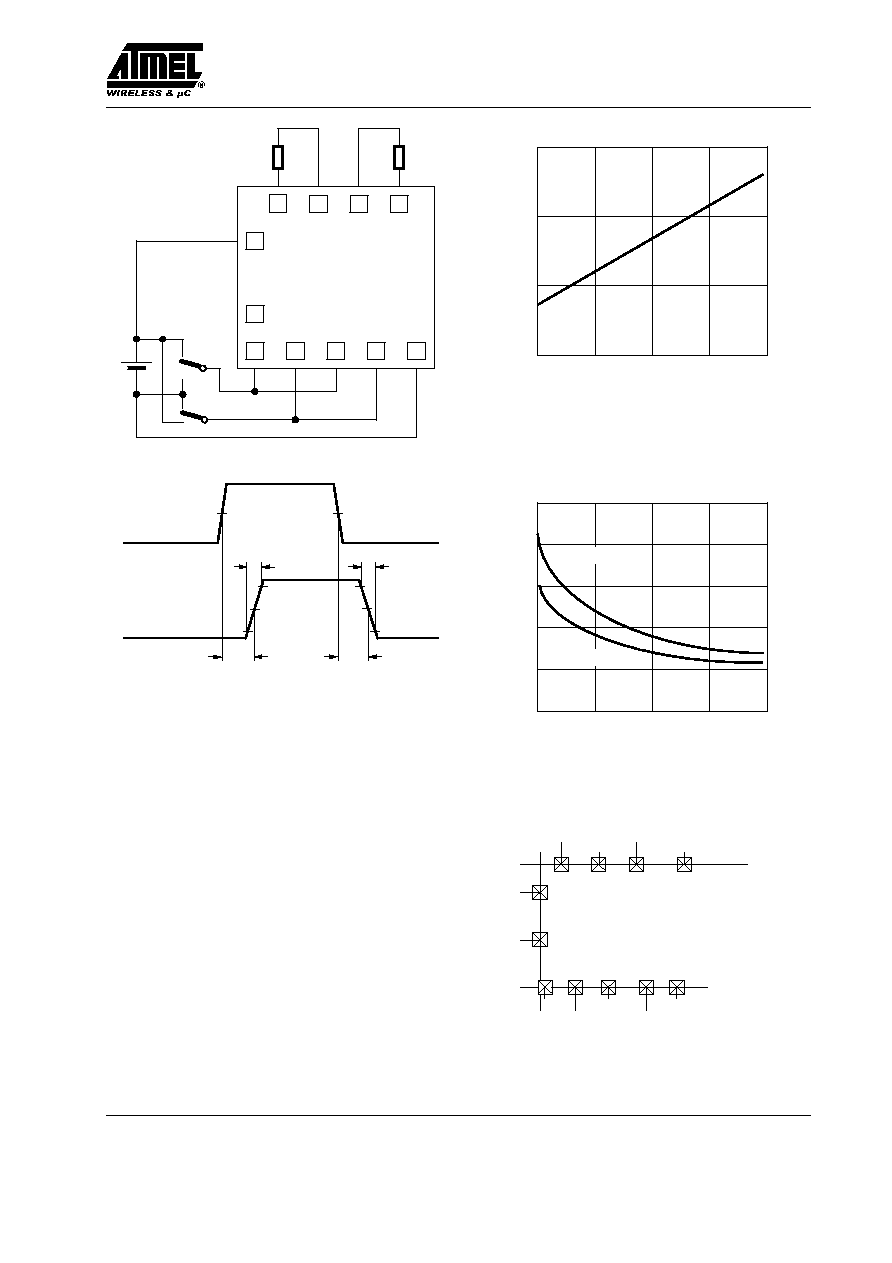
TRI
OUT2
OUT4
OUT3
OUT1
IN3
IN2
IN1
IN4
V
DD
V
SS
e5130
R
L12
R
L34
94 8179
Figure 1. Test circuit
t
Dr
t
Df
t
f
t
r
IN1...4
OUT1...4
94 8181
Figure 2.
Note 1: t
Dr
, t
Df
is defined at 50% of supply voltage
Note 2: t
r
, t
f
is defined from 10% to 90%, resp. 90% to
10% of supply voltage
1.0
1.5
2.0
2.5
0
5
10
15
I ( mA
)
RL
V
DD
( V )
3.0
94 8192
Figure 3. Typical current into 200
W load resistor, condition as
per figure 1
0
10
20
30
40
50
R ( )
ON
V
DD
( V )
94 8193
1.0
1.5
2.0
2.5
3.0
W
N-CH Transistor
P-CH Transistor
Figure 4. Typical output on-resistance vs. supply voltage at
V
DS
= 0.2 V
e5130
1014.0
366.0
534.0
782.0
118.0
0
447.5
851.0
1014.0
0
0
0
778.0
610.0
389.0
221.0
10
94 8180
Figure 5. Pad coordinates
e5130
Rev. A2, 13-Mar-01
4 (4)
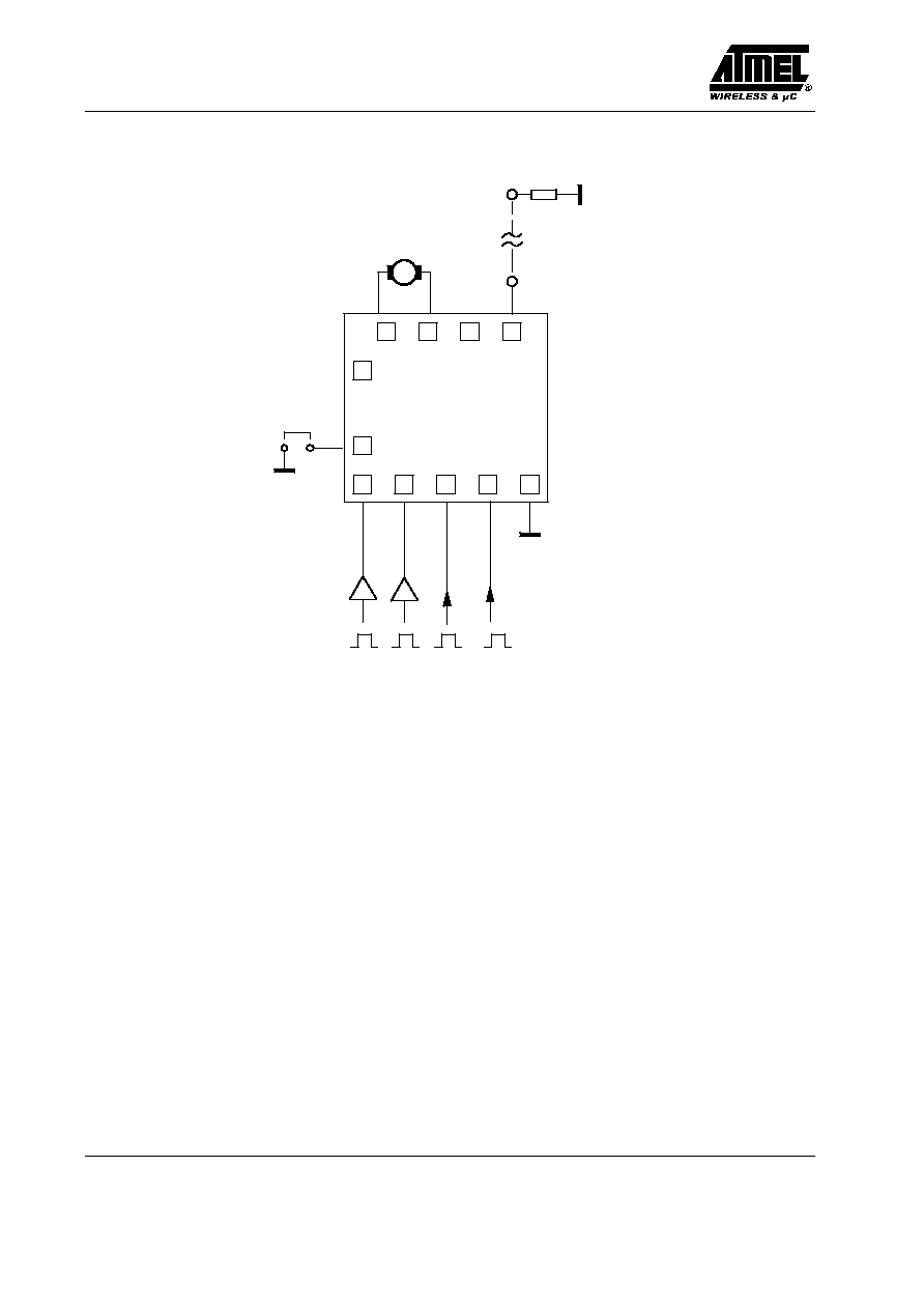
Application Circuit
TRI
OUT2
OUT4
OUT3
OUT1
IN3
IN2
IN1
IN4
V
DD
V
SS
e5130
from logic
or
mP
Line Driver
Load 4.8 mA @ 1.5 V
12 mA @ 3.0 V
M
Micro-Motor or
Stepper Motor
We reserve the right to make changes to improve technical design and may do so without further notice.
Parameters can vary in different applications. All operating parameters must be validated for each customer
application by the customer. Should the buyer use Atmel Wireless & Microcontrollers products for any unintended
or unauthorized application, the buyer shall indemnify Atmel Wireless & Microcontrollers against all claims,
costs, damages, and expenses, arising out of, directly or indirectly, any claim of personal damage, injury or death
associated with such unintended or unauthorized use.
Data sheets can also be retrieved from the Internet: http://www.atmel≠wm.com
Atmel Germany GmbH, P.O.B. 3535, D-74025 Heilbronn, Germany
Telephone: 49 (0)7131 67 2594, Fax number: 49 (0)7131 67 2423