1
Features
∑
16-bit Fixed-point Digital Signal Processing (DSP) Core
∑
Low-power Consumption:
≠ 1 mW/MIPS on 0.25-micron CMOS, 2.5V
≠ 0.6 mW/MIPS on 0.20-micron CMOS, 1.8V
∑
High Performance:
≠ 80 MIPS at 160 MHz (Typical) on 0.25-micron CMOS, 2.5V
≠ 100 MIPS at 200 MHz (Typical) on 0.20-micron CMOS, 1.8V
∑
Small Die Size:
≠ 2.5 mm
2
on 0.25-micron CMOS
≠ 1.3 mm
2
on 0.20-micron CMOS
∑
Slow Mode and Stop Mode allow Further Power Reduction
∑
Wide Range of Operating Voltage: 1.8V - 3.6V
∑
High Level of Modularity:
≠ Expandable Data and Program RAM and/or ROM
≠ User-definable Registers
∑
64K x 16-bit Data Address Space, 64K x 16-bit Program Address Space
∑
Three Parallel Execution Units
∑
Wait States are Supported to Link with Slow External Devices
∑
Advanced Windows-based Development Tools: Macro Assembler, Linker,
C Compiler, Debugger (emulator, simulator)
∑
Optional `On-core Emulator' Allows the On-core Debugger, Embedded in
the ASIC, to be Run
∑
Optional JTAG Serial Interface for On-chip Debug (JCI Interface)
Description
Atmel's embedded OakDSPCore
Æ
is a 16-bit general-purpose low-power, low-voltage
and high-speed digital signal processor (DSP). It is designed for mid-to-high-end tele-
communications and consumer electronics applications, where low power and
portability are major requirements. Among the applications supported are digital cellu-
lar telephones, fast modems, advanced facsimile machines and hard disk drives.
OakDSPCore is available as a DSP core in Atmel's standard cell library, to be utilized
as an engine for DSP-based ASICs. It is specified with several levels of modularity in
RAM, ROM and I/O blocks, allowing efficient DSP-based ASIC development.
OakDSPCore is aimed at achieving the best cost-performance factor for a given
(small) silicon area. As a key element of a system-on-chip, it takes into account such
requirements as program size, data memory size, glue logic, power management, etc.
The OakDSPCore consists of three main execution units operating in parallel: the
Computation/Bit Manipulation Unit (CBU), the Data Address Arithmetic Unit (DAAU)
and the Program Control Unit (PCU). The core also contains ROM and RAM address-
ing units, and Program Control Logic (PCL). All other peripheral blocks, which are
application specific, are defined as a part of the user-specific logic, implemented
around the DSP core on the same silicon die.
OakDSPCore has an enhanced set of DSP and general microprocessor functions to
meet the application requirements. The OakDSPCore programming model and
instruction set are aimed at straightforward generation of efficient and compact code.
Embedded
Digital Signal
Processing
Core
OakDSPCore
Æ
Rev. 0876F≠03/01
3
OakDSPCore
0876F≠03/01
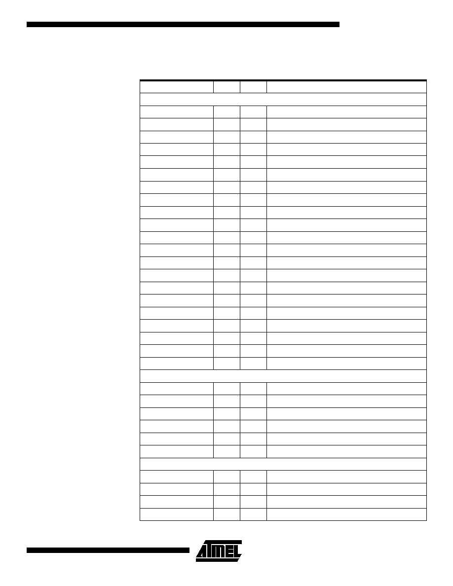
Signal Description
Table 1. Pin Configuration
Signal Name
Size
Type
Description
On-core Memory
RXSP <15:0>
16
I
XRAM data bus
OMEMSZ4P
1
I
Memory size 4K
RYDP <15:0>
16
I
YRAM data bus
GIXDBP <15:0>
16
I/O
Internal data bus
DOCXAP <10:0>
11
O
On-core XRAM address
DOCXA10N
1
O
On-core XRAM address - bit 10
DRXRM1P
1
O
On-core XRAM read (lower 1K)
DWXRM1P
1
O
On-core XRAM write (lower 1K)
DOEXRM1P
1
O
On-core XRAM output enable (lower 1K)
DRXRM2P
1
O
On-core XRAM read (upper 1K)
DWXRM2P
1
O
On-core XRAM write (upper 1K)
DOEXRM2P
1
O
On-core XRAM output enable (upper 1K)
DYAN <10:0>
11
O
On-core YRAM address
DYA10N
1
O
On-core YRAM address - bit 10
DRYRM1P
1
O
On-core YRAM read (lower 1K)
DWYRM1P
1
O
On-core YRAM write (lower 1K)
DOEYRM1P
1
O
On-core YRAM output enable (lower 1K)
DRYRM2P
1
O
On-core YRAM read (upper 1K)
DWYRM2P
1
O
On-core YRAM write (upper 1K)
DOEYRM2P
1
O
On-core YRAM output enable (upper 1K)
PMEMENP
1
O
Data memory enable
Off-core Memory
GEXDBP <15:0>
16
I/O
External data bus
PESRCN <5:0>
6
O
Source bus
PEDSTN <5:0>
6
O
Destination bus
DXAP <15:0>
16
O
Off-core XRAM address
PEDWP
1
O
Data write
PEDRP
1
O
Data read
Program Memory
BEXTPP
1
I
External program indication
GIP <15:0>
16
I/O
Instruction data
PEXTIP
1
O
MOVP instruction indication
PPAP <15:0>
16
O
Program address
5
OakDSPCore
0876F≠03/01
OakDSPCore
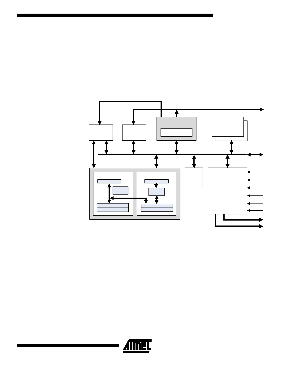
Architecture
As shown in Figure 2, the OakDSPCore consists of three main execution units operating
in parallel:
∑
The Computation/Bit Manipulation Unit (CBU)
∑
The Data Address Arithmetic Unit (DAAU)
∑
The Program Control Unit (PCU)
The OakDSPCore also supports four user-definable registers, enabling future expan-
sion of the core residing in off-core glue logic. The user defined registers are part of the
core register set, meaning that they can be accessed by most OAK instructions.
Figure 2. OakDSPCore Block Diagram
BMU
CU
C B U
P C U
Barrel Shifter
BFO
B-Accumulator 0
B-Accumulator 1
Multiplier
ALU
Accumulator 0
Accumulator 1
DAAU
X-RAM
On-Core Memory
Y-Data Bus
Y-Address Bus
X-Data Bus
X-Address Bus
User
Defined
Register
Stack-Pointer
Y-RAM
Status
Registers
RESET
BPI
INT0
INT1
INT2
NMI
Program Address Bus
Program Data Bus