1
2138D≠HIREL≠06/03
Features
∑
18.1SPECint95, Estimates 12.3 SPECfp95 at 400 MHz (PC755)
∑
15.7SPECint95, 9SPECfp95 at 350 MHz (PC745)
∑
733 MIPS at 400 MHz (PC755) at 641 MIPS at 350 MHz (PC745)
∑
Selectable Bus Clock (12 CPU Bus Dividers up to 10x)
∑
P
D
Typical 6.4W at 400 MHz, Full Operating Conditions
∑
Nap, Doze and Sleep Modes for Power Savings
∑
Superscalar (3 Instructions per Clock Cycle) Two Instruction + Branch
∑
4 Beta Byte Virtual Memory, 4-GByte of Physical Memory
∑
64-bit Data and 32-bit Address Bus Interface
∑
32-KB Instruction and Data Cache
∑
Six Independent Execution Units
∑
Write-back and Write-through Operations
∑
f
INT
max = 400 MHz (TBC)
∑
f
BUS
max = 100 MHz
∑
Voltage I/O 2.5V/3.3V; Voltage Int 2.0V
Description
The PC755 and PC745 PowerPC
Æ
microprocessors are high-performance, low-
power, 32-bit implementations of the PowerPC Reduced Instruction Set Computer
(RISC) architecture, especially enhanced for embedded applications.
The PC755 and PC745 microprocessors differ only in that the PC755 features an
enhanced, dedicated L2 cache interface with on-chip L2 tags. The PC755 is a drop-in
replacement for the award winning PowerPC 750
TM
microprocessor and is footprint
and user software code compatible with the MPC7400 microprocessor with AltiVec
TM
technology. The PC745 is a drop-in replacement for the PowerPC 740
TM
microproces-
sor and is also footprint and user software code compatible with the PowerPC 603e
TM
microprocessor. PC755/745 microprocessors provide on-chip debug support and are
fully JTAG-compliant.
The PC745 microprocessor is pin compatible with the TSPC603e family.
ZF suffix
PBGA255
Flip-Chip Plastic Ball Grid Array
ZF suffix
PBGA360
Flip-Chip Plastic Ball Grid Array
G suffix
CBGA360
Ceramic Ball Grid Array
GH suffix
HITCE 360
Ceramic Ball Grid Array
GS suffix
CI-CGA360
Ceramic Ball Grid Array with
Solder Column Interposer (SCI)
PowerPC
755/745 RISC
Microprocessor
PC755/745
Preliminary
-site
Rev. 2138D≠HIREL≠06/03
2
PC755/745
2138D≠HIREL≠06/03
Screening
This product is manufactured in full compliance with:
∑
CBGA + CI-CGA + FC-PBGA up screenings based upon Atmel standards
∑
HiTCE
∑
Full military temperature range (Tj = -55
∞
C,+125
∞
C)
industrial temperature range (Tj = -40
∞
C,+110
∞
C)
General Description
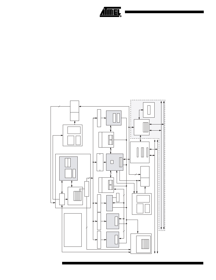
Simplified Block Diagram
The PC755 is targeted for low power systems and supports power management fea-
tures such as doze, nap, sleep, and dynamic power management. The PC755 consists
of a processor core and an internal L2 Tag combined with a dedicated L2 cache inter-
face and a 60x bus.
Figure 1. PC755 Block Diagram
Additional Features
• Time Base Counter/Decrementer
• Clock Multiplier
• JTAG/COP Interface
• Thermal/Power Management
• Performance Monitor
+
+
F
etcher
Branc
h
Pr
ocessing
BTIC
64-Entr
y
+ x ÷
FPSCR
CR
FPSCR
L2CR
CTR
LR
BHT
Data MMU
Instruction MMU
Not in the PC745
EA
PA
+ x ÷
Instruction Unit
Unit
Instr
uction Queue
(6-W
ord)
2 Instructions
Reser
v
ation Station
Reser
v
ation Station
Reser
v
ation Station
Integ
er Unit 1
System Register
Unit
Dispatch Unit
64-Bit
(2 Instr
uctions)
SRs
ITLB
(Shado
w
)
IBA
T
Arr
a
y
32-Kb
yte
I Cache
T
ags
128-Bit
(4 Instr
uctions)
Reser
v
ation Station
32-Bit
Floating-P
o
int
Unit
Rename Buff
ers
(6)
FPR File
32-Bit
64-Bit
64-Bit
Reservation Station
(2-Entry)
Load/Store Unit
(EA Calculation)
Store Queue
GPR File
Rename Buff
ers
(6)
32-Bit
SRs
(Or
i
ginal)
DTLB
DBA
T
Arr
a
y
64-Bit
Completion Unit
Reorder Buff
er
(6-Entr
y)
T
ags
32-Kb
yte
D Cache
60x Bus Interface Unit
Instr
uction F
etch Queue
L1 Castout Queue
Data Load Queue
L2 Contr
o
ller
L2 T
ags
L2 Bus Interface
Unit
L2 Castout Queue
32-Bit Address Bus
32-/64-Bit Data Bus
17-Bit L2 Address Bus
64-Bit L2 Data Bus
Integ
er Unit 2

3
PC755/745
2138D≠HIREL≠06/03
General Parameters
The following list provides a summary of the general parameters of the PC755:
Features
This section summarizes features of the PC755's implementation of the PowerPC archi-
tecture. Major features of the PC755 are as follows:
∑
Branch Processing Unit
≠
Four instructions fetched per clock
≠
One branch processed per cycle (plus resolving 2 speculations)
≠
Up to 1 speculative stream in execution, 1 additional speculative stream in
fetch
≠
512-entry branch history table (BHT) for dynamic prediction
≠
64-entry, 4-way set associative Branch Target Instruction Cache (BTIC) for
eliminating branch delay slots
∑
Dispatch Unit
≠
Full hardware detection of dependencies (resolved in the execution units)
≠
Dispatch two instructions to six independent units (system, branch,
load/store, fixed-point unit 1, fixed-point unit 2, floating-point)
≠
Serialization control (predispatch, postdispatch, execution serialization)
∑
Decode
≠
Register file access
≠
Forwarding control
≠
Partial instruction decode
∑
Completion
≠
6 entry completion buffer
≠
Instruction tracking and peak completion of two instructions per cycle
≠
Completion of instructions in program order while supporting out-of-order
instruction execution, completion serialization and all instruction flow
changes
∑
Fixed Point Units (FXUs) that share 32 GPRs for Integer Operands
≠
Fixed Point Unit 1 (FXU1)-multiply, divide, shift, rotate, arithmetic, logical
≠
Fixed Point Unit 2 (FXU2)-shift, rotate, arithmetic, logical
Technology
0.22 µm CMOS, six-layer metal
Die size
6.61 mm x 7.73 mm (51 mm
2
)
Transistor count
6.75 million
Logic design
Fully-static Packages
PC745
Surface mount 255 Plastic Ball Grid Array (PBGA)
PC755
Surface mount 360 Plastic Ball Grid Array (PBGA)
Surface mount 360 Ceramic Ball Grid Array (CI-CGA, CBGA,
HiTCE)
Core power supply
2V ± 100 mV DC (nominal; some parts support core voltages
down to 1.8V; see Table 5 for recommended operating
conditions)
I/O power supply
2.5V ± 100 mV DC or 3.3V ± 165 mV DC (input thresholds are
configuration pin selectable)

4
PC755/745
2138D≠HIREL≠06/03
≠
Single-cycle arithmetic, shifts, rotates, logical
≠
Multiply and divide support (multi-cycle)
≠
Early out multiply
∑
Floating-point Unit and a 32-entry FPR File
≠
Support for IEEE-754 standard single and double precision floating point
arithmetic
≠
Hardware support for divide
≠
Hardware support for denormalized numbers
≠
Single-entry reservation station
≠
Supports non-IEEE mode for time-critical operations
∑
System Unit
≠
Executes CR logical instructions and miscellaneous system instructions
≠
Special register transfer instructions
∑
Load/Store Unit
≠
One cycle load or store cache access (byte, half-word, word, double-word)
≠
Effective address generation
≠
Hits under misses (one outstanding miss)
≠
Single-cycle unaligned access within double word boundary
≠
Alignment, zero padding, sign extend for integer register file
≠
Floating point internal format conversion (alignment, normalization)
≠
Sequencing for load/store multiples and string operations
≠
Store gathering
≠
Cache and TLB instructions
≠
Big and Little-endian byte addressing supported
≠
Misaligned Little-endian supported
≠
Level 1 Cache structure
≠
32K, 32 bytes line, 8-way set associative instruction cache (iL1)
≠
32K, 32 bytes line, 8-way set associative data cache (dL1)
≠
Cache locking for both instruction and data caches, selectable by group of
ways
≠
Single-cycle cache access
≠
Pseudo least-recently used (PLRU) replacement
≠
Copy-back or Write Through data cache (on a page per page basis)
≠
Supports all PowerPC memory coherency modes
≠
Non-Blocking instruction and data cache (one outstanding miss under hits)
≠
No snooping of instruction cache
∑
Level 2 (L2) Cache Interface (not implemented on PC745)
≠
Internal L2 cache controller and tags; external data SRAMs
≠
256K, 512K, and 1-Mbyte 2-way set associative L2 cache support
≠
Copyback or write-through data cache (on a page basis, or for all L2)
≠
Instruction-only mode and data-only mode.
≠
64 bytes (256K/512K) or 128 bytes (1M) sectored line size

5
PC755/745
2138D≠HIREL≠06/03
≠
Supports flow through (register-buffer) synchronous burst SRAMs, pipelined
(register-register) synchronous burst SRAMs (3-1-1-1 or strobeless 4-1-1-1)
and pipelined (register-register) late-write synchronous burst SRAMs
≠
L2 configurable to direct mapped SRAM interface or split cache/direct
mapped or private memory
≠
Core-to-L2 frequency divisors of 1, 1.5, 2, 2.5, and 3 supported
≠
64-bit data bus
≠
Selectable interface voltages of 2.5V and 3.3V
≠
Parity checking on both L2 address and data
∑
Memory Management Unit
≠
128 entry, 2-way set associative instruction TLB
≠
128 entry, 2-way set associative data TLB
≠
Hardware reload for TLBs
≠
Hardware or optional software tablewalk support
≠
8 instruction BATs and 8 data BATs
≠
8 SPRGs, for assistance with software tablewalks
≠
Virtual memory support for up to 4 hexabytes (2
52
) of virtual memory
≠
Real memory support for up to 4 gigabytes (2
32
) of physical memory
∑
Bus Interface
≠
Compatible with 60X processor interface
≠
32-bit address bus
≠
64-bit data bus, 32-bit mode selectable
≠
Bus-to-core frequency multipliers of 2x, 3x, 3.5x, 4x, 4.5x, 5x, 5.5x, 6x, 6.5x,
7x, 7.5x, 8x, 10x supported
≠
Selectable interface voltages of 2.5V and 3.3V.
≠
Parity checking on both address and data busses
∑
Power Management
≠
Low-power design with thermal requirements very similar to PC740/750.
≠
Selectable interface voltage of 1.8V/2.0V can reduce power in output buffers
(compared to 3.3V)
≠
Three static power saving modes: doze, nap, and sleep
≠
Dynamic power management
∑
Testability
≠
LSSD scan design
≠
IEEE 1149.1 JTAG interface
∑
Integrated Thermal Management Assist Unit
≠
One-ship thermal sensor and control logic
≠
Thermal Management Interrupt for software regulation of junction
temperature