 | –≠–ª–µ–∫—Ç—Ä–æ–Ω–Ω—ã–π –∫–æ–º–ø–æ–Ω–µ–Ω—Ç: T0345 | –°–∫–∞—á–∞—Ç—å:  PDF PDF  ZIP ZIP |

1 (18)
Preliminary Information
Features
∑
Low 2.7 V supply-voltage
∑
Single sideband upconverters
∑
100 dB control range
∑
Low current consumption
∑
Individual block power down capability
∑
On-chip IF PLL
∑
3-wire bus programming
∑
Full ESD protection
Benefits
∑
Extended battery-operating time
∑
Few external components
∑
VCO control without voltage doubler
∑
One device for dual band cellular/PCS and dual mode CDMA/AMPS operation
∑
Only single IF-filter for all 3 modes
∑
Very small MLF32 package
∑
Simple 4-bit programming
∑
Excellent linearity
∑
Low current consumption
∑
Very high output power
Electrostatic sensitive device.
Observe precautions for handling.
Description
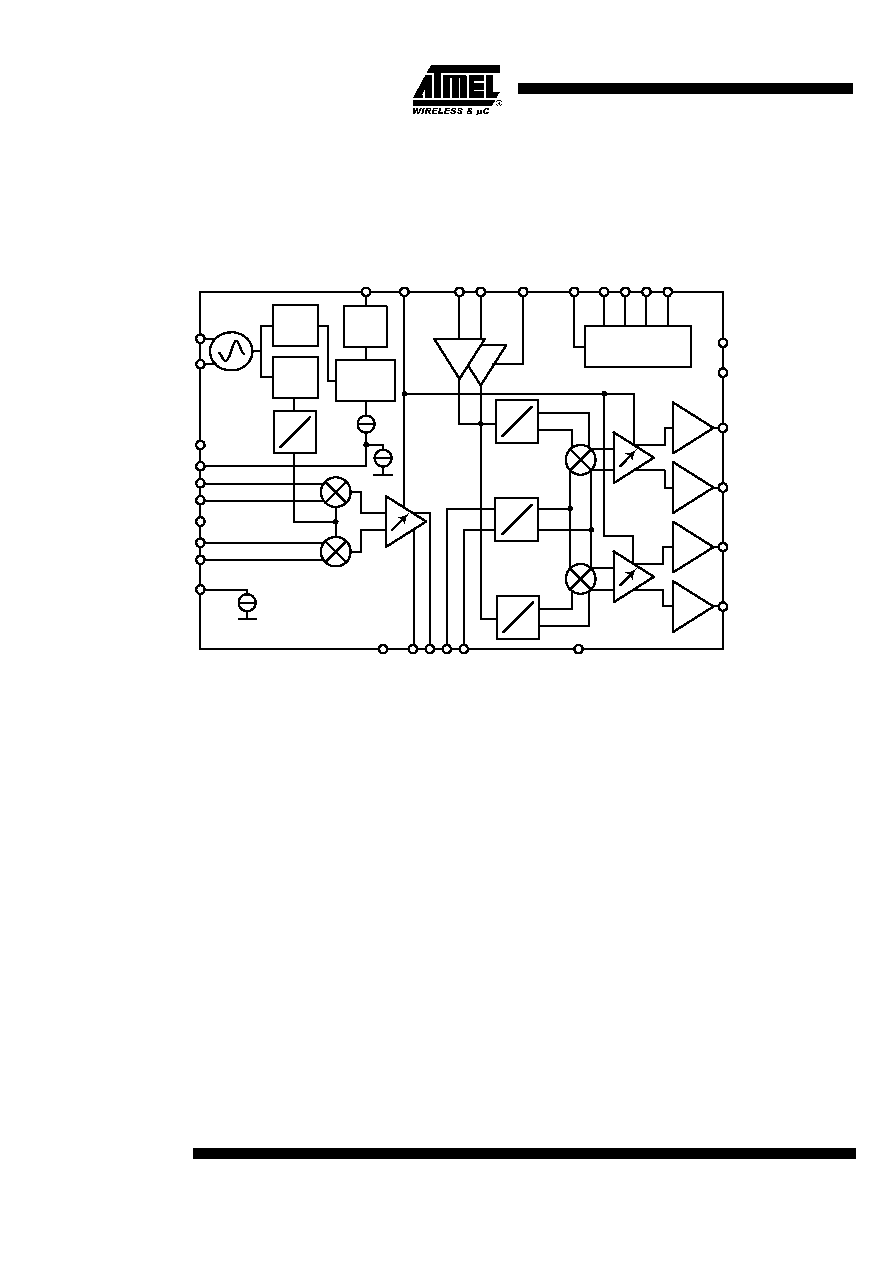
T0345 is a monolithic integrated circuit, realised using Atmel Wireless & Microcontrol-
lers advanced silicon germanium bipolar SiGe technology. Its RF performance meets
the requirements for products designed to IS-95/98 standards. It incorporates the
complete transmitter chain for dual-band triple-mode cellular phones supporting
CDMA (IS95) in cellular and PCS bands as well as AMPS. The device integrates an
I/Q modulator, variable gain amplifier (VGA), two single side-band up-conversion
mixer with fully integrated LO phase shifters, a voltage-controlled oscillator (VCO).
Furthermore it includes a complete PLL with dividers, phase-frequency detector (PFD)
and a charge pump. T0345 provides programmable output power in cellular and PCS
band. The IC is available in a small leadless micro lead frame outline 32-pin (MLF32)
package.
Ordering Information
Extended Type Number
Package
Remarks
T0345
MLF32
Dual Band
CDMA / AMPS
Transmitter
T0345
Rev. A3, 21-Nov-01
2 (18)
Preliminary Information
T0345
Rev. A3, 21-Nov-01
Block Diagram
Figure 1.
Phase
Detector
/4
/53
PCS_LO
TCX
O
/2
0∞
0∞
90∞
Cell_LO
Vc
c
VCO T1
VCO T2
Vc
c
_bus
CL
DA
EN
LPF
I+
I-
Q+
Q-
V
CNTRL
0∞
0∞
90∞
Control
D
r
v
_
SEL
0∞
0∞
90∞
IF_O
UT(
-
)
IF_O
UT(
+
)
UP
_IN(-)
UP
_IN(+
)
PCSB
PCSA
CellB
CellA
Vcc
TX ON
Vc
c
Vcc
Vcc
Vc
c
1
2
3
4
5
6
7
8
9
10 11 12
13
14
15
16
32
18
19
20
21
23
22
24
25
26
27
28
29
30
31
17
Iref
0∞
0∞
90∞
3 (18)
Preliminary Information
T0345
Rev. A3, 21-Nov-01
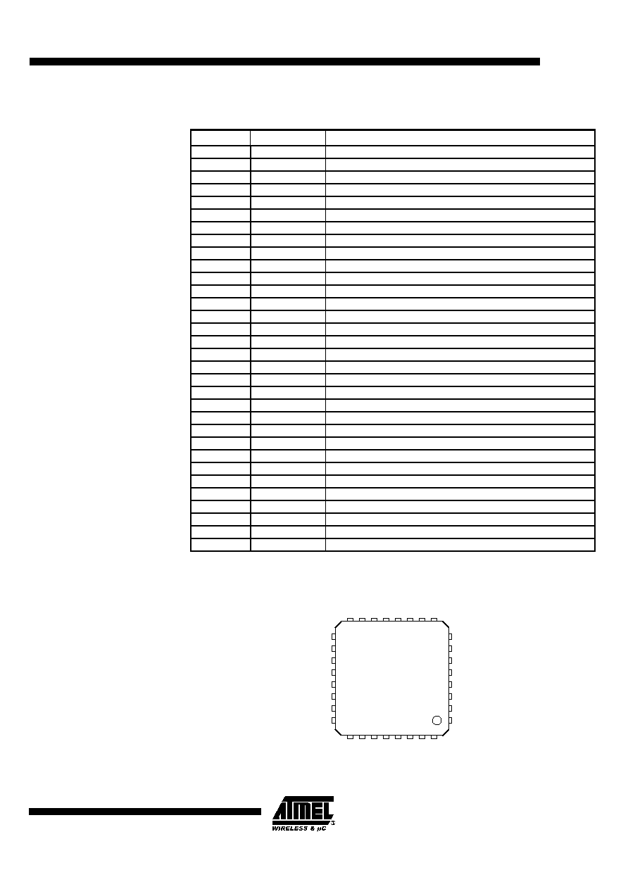
Figure 2. Pinning
Pin Description
Pin
Symbol
Function
1
Cell_LO
Local oscillator cellular 900 MHz input
2
PCS_LO
Local oscillator PCS 1800 MHz input
3
VCC
Supply voltage
4
TCXO
TCXO input
5
VCC
Supply voltage
6
LPF
Charge pump loop filter
7
VCO_T1
Voltage controlled oscillator external tank circuit
8
VCO_T2
Voltage controlled oscillator external tank circuit
9
VCC_bus
Supply voltage for serial bus interface
10
CL
3-wire bus, clock input
11
DA
3-wire bus, data input
12
EN
3-wire bus, enable strobe input
13
I+
I+ data differential signal input
14
I-
I- data differential signal input
15
Q+
Q+ data differential signal input
16
Q-
Q- data differential signal input
17
Iref
Constant current sink
18
IF_OUT(-)
Output to IF filter
19
IF_OUT(+)
Output to IF filter
20
UP_IN(+)
Input from IF filter
21
UP_IN(-)
Input from IF filter
22
VCC
Supply RF mixer supply voltage
23
VCC
Supply RF VGA supply voltage
24
VCNTRL
Gain control analog voltage input
25
TX ON
Transmitter ON (= high), power up logic control signal
26
CELLB
Cell band driver amplifier B output, open collector
27
CELLA
Cell band driver amplifier A output, open collector
28
VCC
Supply voltage
29
PCSB
PCS band driver amplifier B output, open colletor
30
PCSA
PCS band driver amplifier A output, open colletor
31
DRV_SEL
Driver select logic control input
32
Vcc
Supply voltage
Iref
IF_OUT-
IF_OUT+
UP_IN+
UP_IN-
Vcc
Vcc
VCNTRL
VCO_T2
VCO_T1
LPF
Vcc
TCXO
VCC
PCS_LO
Cell_LO
Q-
Q+
I-
I+
EN
DA
CL
Vcc_
Bu
s
TX_ON
CE
LLB
CE
LLA
VC
C
PC
SB
PC
SA
DRV
_S
E
L
Vcc
16 15 14 13 12 11 10 9
25 26 27 28 29 30 31 32
17
18
19
20
21
22
23
24
8
7
6
5
4
3
2
1

4 (18)
Preliminary Information
T0345
Rev. A3, 21-Nov-01
Absolute Maximum Ratings
Parameter
Symbol
Value
Unit
Supply voltages Vcc
V
CC
4.0
V
Voltage at any input
V
Vi
-0.5
V
Vi
V
VCC
+0.5
V
Current at any input/output pin
I
I#
,
I
O#
40mA
mA
Case temperature
T
C
-30 to + 85
∞C
Storage temperature
T
stg
-40 to +150
∞C
Thermal Resistance
Parameter
Symbol
Value
Unit
Junction-ambient MLF32
R
thJA
t.b.d.
K/W
Operating Range
Parameter
Symbol
Value
Unit
Supply voltage
V
cc
2.7
to
3.3
V
Case temperature
T
C
-30 to +85
∞C
5 (18)
Preliminary Information
T0345
Rev. A3, 21-Nov-01
Electrical Characteristics: DC Supply
Test conditions:V
CC
= 3.00 VDC, Tc = 25∞C unless otherwise specified. Min./Max. limits are at +25∞C case temperature unless otherwise
specified. Atmel Wireless & Microcontrollers' test board.
No.
Parameters
Test Conditions
Pin
Symbol
Min.
Typ.
Max.
Unit
Type*
1
Supply
1.1
Supply voltages
3, 5,
22,
23,
28, 32
V
CC
2.7
3.3
VDC
D
1.2
Cell band mode
current consumption
(Driver A or Driver B
activated)
High power
(Pwr_up = 1, Bit1 = 0,
Bit2 = 0,
AB_SEL = high or low,
Pout = 7.7 dBm)
Low power
(Pwr_up = 1, Bit1 = 0,
Bit2 = 0,
AB_SEL = high or low,
Pout = -90 dBm)
103
90
mA
mA
C
1.3
PCS band mode
current consumption
(Driver A or Driver B
activated)
High power
(Pwr_up = 1, Bit1 = 1,
Bit2 = 0,
AB_SEL = high or low,
Pout = 8.2 dBm)
Low power
(Pwr_up = 1, Bit1 = 1,
Bit2 = 1,
AB_SEL = high or low,
Pout = -90 dBm)
103
90
mA
mA
C
1.4
Cell band mode
current consumption
(Driver A and Driver B
activated)
High power
(Pwr_up = 1, Bit1 = 0,
Bit2 = 1,
Pout = 10.7 dBm)
Low power
(Pwr_up = 1, Bit1 = 0,
Bit2 = 1,
Pout = -87 dBm)
120
90
mA
mA
C
1.5
PCS band mode
current consumption
(Driver A and Driver B
activated)
High power
(Pwr_up = 1, Bit1 = 1,
Bit2 = 1,
Pout = 11 dBm)
Low power
(Pwr_up = 1, Bit1 = 1,
Bit2 = 1,
Pout = -87 dBm)
120
90
mA
mA
C
*) Type means: A =100% tested, B = 100% correlation tested, C = Characterized on samples, D = Design parameter