 | –≠–ª–µ–∫—Ç—Ä–æ–Ω–Ω—ã–π –∫–æ–º–ø–æ–Ω–µ–Ω—Ç: T0352 | –°–∫–∞—á–∞—Ç—å:  PDF PDF  ZIP ZIP |

1
Features
∑
KPCS Band CDMA and GPS Operation
∑
Low Current Consumption
∑
Excellent Noise and IP3 Performance
∑
Adjustable Third Order Intercept on LNA Stage
∑
Flexible IF Frequency Range from 80 MHz to 230 MHz
∑
Excellent Cross Modulation Performance
Applications
∑
Quad-mode/Dual-band CDMA IS-95/98 Based Mobile Phones with GPS Support
∑
Other Familiar Applications
Benefits
∑
High Linearity Eliminates Potential Call Drop Issues Associated with Gain Switching
∑
Most Compact Integrated Receiver for K-PCS and A-GPS Applications
∑
IM98 IMD Requirements Met with two Gain States Simplifying Calibration Procedure
∑
Best in Class A-GPS CascadeGgain for Maximum Take-over
∑
TX LO Buffer Included
∑
Few External Components
∑
Fully ESD Protected
Electrostatic sensitive device.
Observe precautions for handling.
Description
The T0352 is a CDMA front-end receiver RFIC designed for dual-band, dual-mode
operation. The device supports Korean PCS (K-PCS) CDMA and A-GPS operation.
The IF range is from 80 MHz to 230 MHz with external tuning. The K-PCS low noise
amplifier has an adjustable third order intercept (IP3) to minimize inter-modulation and
cross-modulation effects. The mixers are designed for differential IF outputs (single-
ended or differential IF outputs for GPS modes), and they feature excellent linearity
and low noise figure.
The T0352 device is available in a 4 mm
¥
4 mm MLF package with 24 pins. This
front-end receiver is capable of meeting all electrical requirements in accordance with
the TIA/EIA 98-C Wireless Communication standard.
2.8 V Dual-band/
Dual-mode RF
Receiver for
K-PCS/GPS
T0352
Preliminary
(Summary)
Rev. 4579AS≠CDMA≠11/02

2
T0352
4579AS≠CDMA≠11/02
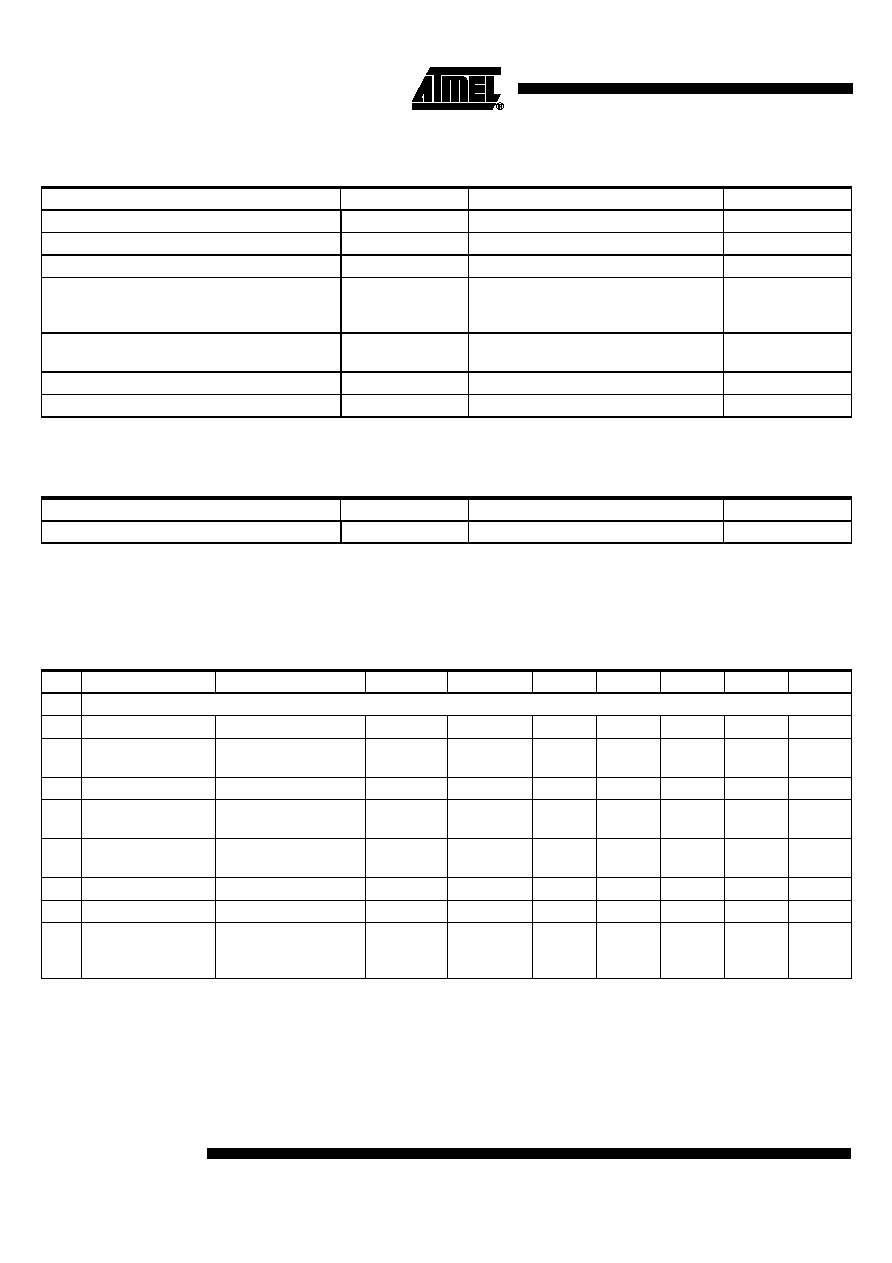
Figure 1. Block Diagram
Pin Configuration
Figure 2. Pinning HP-VFQFP-N24
PLO_IN
BUFFEN
PCS_On
LIN/GPS
Con
t
r
o
l
PLNA_IN
PLO_Out
PCS_Out+
PCS_Out-
P
L
NA
_
O
UT
PMi
x
_
I
N
P
L
NA
_
G
ND
Is
e
t
_
P
C
S
2
3
24
20
1
21
23
22
18
17
12
8
GLNA_IN
GMix_Out+
GMix_Out-
GM
ix
_I
N
GL
NA
_O
ut
Vc
c_
Mi
x
5
7
11
15
14
13
Vcc_Dig
GLO_IN
9
Vc
c_
L
N
A
4
Vcc_LO
6
19
ISET_PCS
PLNA_IN
VCC_LNA
GLNA_IN
GND
VCC_LO
PMix_O+
PMix_O-
GND
VCC_ MIX
GMix_Out-
P
L
NA
_O
UT
PC
S_
O
N
LI
N/
GP
S
BU
FFEN
PMix_
I
N
V
CC_DIG
GLNA_OUT
PL
O
_
IN
GL
O_I
N
GND
GM
ix
_I
N
PL
O
_
O
U
T
24 23 22 21 20 19
7 8 9 10 11 12
18
17
16
15
14
13
1
2
3
4
5
6
GMix_Out+
3
T0352
4579AS≠CDMA≠11/02
Pin Description
Pin
Symbol
Function
1
Iset_PCS
Bias resistor for K-PCS LNA. For typical bias use a 560
W
resistor to ground which set the bias current
for HGHL mode.
2
PLNA_IN
PCS LNA input. Requires a DC blocking capacitor and an L-C (shunt C/series L) matching network for
optimum gain, intercept and noise performance.
3
Vcc_LNA
Power supply pin for K-PCS LNA. Bypass with a capacitor as close to the pin as possible.
4
GLNA_IN
GPS LNA input. Requires LC match, see Pin 2.
5
GLNA_GND
GPS LNA emitter-ground. The LNA emitter ground should be grounded immediately to the ground
plane to reduce stray inductance and capacitance that may affect performance.
6
Vcc_LO
Supply voltage for LO buffer.
7
GLNA_OUT
GPS LNA output
.
8
PLO_IN
K-PCS LO input.
9
GLO_IN
GPS LO input.
10
GND
Device ground.
11
GMix_IN
GPS mixer input.
12
PLO_OUT
K-PCS LO buffer output. Internally matched to 100
W
. Does not require a blocking capacitor.
13
GMix_OUT-
Negative GPS IF output.
14
GMix_OUT+
Positive GPS IF output.
15
Vcc_Mix
Supply voltage for all mixers.
16
GND
Device ground.
17
PMix_OUT-
Negative CDMA IF output.
18
PMix_OUT+
Positive CDMA IF output.
19
Vcc_DIG
Supply voltage for logic control circuits.
20
PMix_IN
K-PCS Mixer RF input.
21
BUFFEN
LO output buffer enable. Set BUFFEN pin HIGH to power up the PCS LO buffer output.
22
LIN/GPS
≠
23
PCS_ON
Logic input for activating PCS LNA; Logic high selects PCS. Logic low
means inactive.
24
PLNA_OUT
PCS LNA output. Requires a pull-up inductor to Vcc and a series blocking capacitor, which can be
used as the output matching network.
≠
Paddle
Device ground and heat sink, requires good thermal path; RF reference plane.
4
T0352
4579AS≠CDMA≠11/02
Absolute Maximum Ratings
Parameters
Symbol
Value
Unit
Supply voltages, no RF applied
V
CC
-0.5 to +4.0
V
Logic control voltages
V
CTRL
-0.5 to + V
CC
+0.5
V
Supply current
I
CC
50.0
mA
RF and LO input signals
P
LO ;
G
LO;
PLNA_IN;
GLNA_IN;
5.0 dBm
I
SET_PCS
; I
SET_CELL
LNA IP3
Adjustment
1
mA
Operating case temperature
T
C
-40 to +100
∞C
Storage temperature
T
STG
-55 to +150
∞C
Thermal Resistance
Parameters
Symbol
Value
Unit
Junction ambient
R
thJA
TBD
K/W
DC Supply Characteristics
Test conditions: Unless otherwise noted, the following conditions apply to typical performance specification under static
conditions (no RF applied): V
CC
= +2.75 V, T
amb
= 25∞C.
No.
Parameters
Test Conditions
Pin
Symbol
Min.
Typ.
Max.
Unit
Type*
All Modes
Supply voltage
3, 15, 19
V
CC
2.7
2.8
3.3
V
Control voltage
high
23, 21, 22
V
CTRL
1.7
V
Control voltage low
21, 22, 23
V
CTRL
0.5
V
LO Rx buffer
supply current
15
I
CC_MIX
7.0
mA
LO Tx buffer
current
BUFFEN = High
15
I
CC_MIX
6.0
mA
Logic-high current
21, 22, 23
I
CTRL
100
µ
A
Logic-low current
21, 22, 23
I
CTRL
-5.0
µ
A
Power-down
supply current
PCS_On, LIN = Low
3, 13, 14,
15, 17, 18,
19, 24
I
CC
10
µA
*) Type means: A = 100% tested, B = 100% correlation tested, C = Characterized on samples, D = Design parameter
5
T0352
4579AS≠CDMA≠11/02
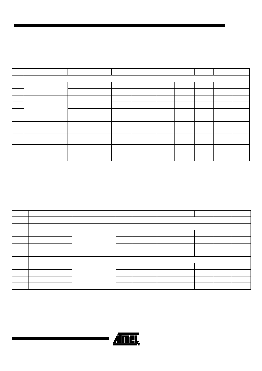
AC Electrical Characteristics
Test conditions: Unless otherwise noted, the following conditions apply to typical performance specification under static
conditions: V
CC
= +2.75 V, T
amb
= 25∞C, all RF inputs and outputs with a return loss of 10 dB minimum.
No.
Parameters
Test Conditions
Pin
Symbol
Min.
Typ.
Max.
Unit
Type*
General Performance
Operating frequency
range
K-PCS band
2, 20
f
PCS
1840
1855
1870
MHz
A-GPS band
4, 11
f
GPS
1575.42
MHz
LO frequency range
K-PCS band:
IF = 183.6 MHz
8
f
LOPCS
1656
1686
MHz
8
f
LOPCS
2023
2053
MHz
GPS band:
IF = 183.6 MHz
9
f
LOGPS
1391.82
MHz
9
f
LOGPS
1759.02
MHz
IF frequency range
K-PCS and GPS
Band
13, 14,
17, 18
f
IF
80
85
230
MHz
LO input power level
K-PCS and GPS
Band
8, 9
P
LO
-10
-5
0
dBm
LO Tx buffer output
power level
K-PCS band; not
matched at dedicated
frequency
12
P
LOOUT
-8
-3
dBm
*) Type means: A = 100% tested, B = 100% correlation tested, C = Characterized on samples, D = Design parameter
Cascade RF Electrical Characteristics (K-PCS Band)
Test conditions: Unless otherwise noted, the following conditions apply to typical performance specification under static
conditions: V
CC
= +2.75 V, T
amb
= 25∞C, RF = 1960 MHz; LO = 2045 MHz; IF = 85 MHz; LO input = -5.0 dBm; RF input = -
30 dBm (high gain mode)
No.
Parameters
Test Conditions
Pin
Symbol
Min.
Typ.
Max.
Unit
Type*
Combined LNA and Mixer Performance (CDMA Modulation)
High-gain High-linearity Mode (HGHL)
Gain
PCS_On = High;
LIN = High
G
26
dB
Noise figure
NF
2.2
dB
Input IP3
IIP3
-1.5
dBm
Supply current
I
CC
30
mA
High-gain Low-linearity Mode (HGLL, Paging Mode)
Gain
PCS_On = High;
LIN = Low
G
25.3
dB
Noise figure
NF
2.2
dB
Input IP3
IIP3
-5.3
dBm
Supply current
I
CC
24
mA
*) Type means: A = 100% tested, B = 100% correlation tested, C = Characterized on samples, D = Design parameter