 | –≠–ª–µ–∫—Ç—Ä–æ–Ω–Ω—ã–π –∫–æ–º–ø–æ–Ω–µ–Ω—Ç: T0781-6C | –°–∫–∞—á–∞—Ç—å:  PDF PDF  ZIP ZIP |
1
Features
∑
Active Mixer with Conversion Gain
∑
No External LO Driver Necessary
∑
Low LO Drive Level Required
∑
RF and LO Ports May Be Driven Single-ended
∑
Single 5-V Supply Voltage
∑
High LO-RF Isolation
∑
Broadband Resistive 50-
W
Impedances on All Three Ports
Applications
∑
Infrastructure Digital Communication Systems
∑
1700 MHz to 2300 MHz Receivers for CDMA/PCS/DCS/UMTS Base Stations
Electrostatic sensitive device.
Observe precautions for handling.
Description
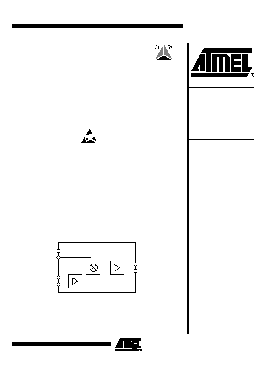
The T0781 is a high linearity active mixer which is manufactured using Atmel's
advanced Silicon-Germanium technology. This mixer features a frequency range of
1700 MHz to 2300 MHz. It operates from a single 5-V supply and provides 12 dB of
conversion gain while requiring only 0 dBm input to the integrated LO driver. An IF
amplifier is also included.
The T0781 incorporates internal matching on each RF, IF and LO ports to enhance
ease of use and to reduce the external components required. The RF and LO inputs
can be driven differentially or single-ended.
Figure 1. Block Diagram
IFP
IFN
LOP
LON
RFP
RFN
4
5
13
1
16
12
1700 - 2300 MHz
High Linearity
SiGe Active
Receiver Mixer
T0781
Preliminary
Rev. 4534B≠SIGE≠01/03
2
T0781
4534B≠SIGE≠01/03
Pin Configuration
Figure 2. Pinning SSOP16
IFN
VCC
GND
LOP
LON
GND
VCC
L2
1
2
3
4
5
6
7
8
16
15
14
13
12
11
10
9
IFP
VCC
GND
RFP
RFN
GND
VCC
L1
Pin Description
Pin
Symbol
Function
1
IFP
IF positive output
2
VCC
5-V power supply
3
GND
Ground
4
RFP
RF positive input
5
RFN
RF negative input
6
GND
Ground
7
VCC
5-V power supply
8
L1
External inductor terminal
9
L2
External inductor terminal
10
VCC
5-V power supply
11
GND
Ground
12
LON
Local oscillator, negative input
13
LOP
Local oscillator, positive input
14
GND
Ground
15
VCC
5-V power supply
16
IFN
IF negative output
3
T0781
4534B≠SIGE≠01/03
Absolute Maximum Ratings
(1)
All voltages are referred to GND.
Parameters
Symbol
Value
Unit
Supply voltage
V
CC
5.5
V
LO input
LOP, LON
10
dBm
IF input
RFP, RFN
15
V
Operating temperature
T
OP
-40 to +85
∞C
Storage temperature
T
stg
-65 to +150
∞C
Notes: 1. The device may not survive all maximum values applied simultaneously.
Thermal Resistance
Parameters
Symbol
Value
Unit
Junction ambient
R
thJA
TBD
K/W
Junction case
R
thJC
46
∞C/W
Electrical Characteristics
Test Conditions: V
CC
= 5 V, T
amb
= 25∞C, RF input: -40 dB at 1880 MHz, LO input: 0 dBm at 1680 MHz
No.
Parameters
Test
Conditions
Pin
Symbol
1700 to 2000 MHz
Operation
2000 to 2300 MHz
Operation
Unit
Type*
Min.
Typ.
Max.
Min.
Typ.
Max.
1
AC Performance
1.1
RF frequency
range
For RF = 2000
to 2300 MHz
operation,
single-ended
RF + LO drive is
recommended
4, 5
f
RF
1700
2000
2000
2300
MHz
B, C
1.11
LO frequency
range
f
LO
1400
2000
1700
2300
MHz
B, C
1.2
IF frequency
range
1,
16
F
IF
30
200
300
30
200
300
MHz
B, C
1.3
Input IP3
RF1 = RF2 =
-15 dBm/tone,
1 MHz spacing
4, 5
IIP3
12
15
12
15
dBm
D
1.4
Input P1dB
4, 5
P1dB
1
2
3
5
dBm
D
1.5
Conversion gain
1,
16
G
9
12
6
9
dB
A
*) Type means: A = 100% tested, B = 100% correlation tested, C = Characterized on samples, D = Design parameter
Note:
1. The return losses shown were measured with the T0781 mounted on Atmel's FR4 evaluation boards using standard
matching practices as indicated on the respective application schematic (see Figure 23 and Figure 24). Users following
the RF, LO and IF matching guidelines will achieve similar performance.
4
T0781
4534B≠SIGE≠01/03
1.6
SSB noise figure
1,
16
NF
SSB
14
15
16
19
dB
D
1.7
RF return loss
Matched to
50
W
(1)
4, 5
RL
RF
20
20
dB
D
1.8
LO return loss
Matched to
50
W
(1)
12,
13
RL
LO
20
20
dB
D
1.9
IF return loss
Matched to
50
W
(1)
1,
16
RL
IF
20
20
dB
D
1.10
LO drive
Matched to
50
W
12,
13
P
LO
-3
0
+3
-3
0
+3
dBm
D
2
Isolation Performance
2.1
Leakage (LO-RF)
12,
13
A
LO-RF
-60
-40
-30
-20
dBm
D
2.2
Leakage (LO-IF)
12,
13
A
LO-IF
-30
-20
-30
-20
dBm
D
2.3
Leakage (RF-IF)
-53
-40
-35
-25
dBm
D
3
Miscellaneous
3.1
Supply voltage
2,
7,
10,
15
V
CC
4.75
5.0
5.25
4.75
5.0
5.25
V
A
3.2
Supply current
2,
7,
10,
15
I
CC
160
180
160
180
mA
A
Electrical Characteristics (Continued)
Test Conditions: V
CC
= 5 V, T
amb
= 25∞C, RF input: -40 dB at 1880 MHz, LO input: 0 dBm at 1680 MHz
No.
Parameters
Test
Conditions
Pin
Symbol
1700 to 2000 MHz
Operation
2000 to 2300 MHz
Operation
Unit
Type*
Min.
Typ.
Max.
Min.
Typ.
Max.
*) Type means: A = 100% tested, B = 100% correlation tested, C = Characterized on samples, D = Design parameter
Note:
1. The return losses shown were measured with the T0781 mounted on Atmel's FR4 evaluation boards using standard
matching practices as indicated on the respective application schematic (see Figure 23 and Figure 24). Users following
the RF, LO and IF matching guidelines will achieve similar performance.
5
T0781
4534B≠SIGE≠01/03
1700 MHz to 2000 MHz: Typical Device Performance
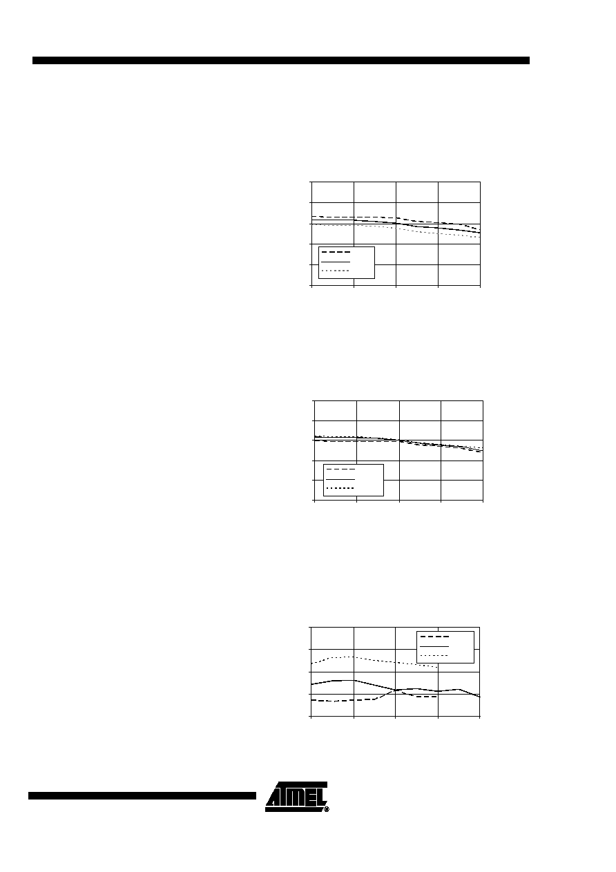
Figure 3. Conversion Gain Versus Temperature, P
LO
= 0 dBm
Figure 4. Conversion Gain Versus LO Drive, T
amb
= 25
∞
C
Figure 5. Leakages, P
LO
= 0 dBm at Pins, P
RF
= -20 dBm at Pins, T
amb
= 25
∞
C
Conversion Gain vs Temperature
Plo = 0dBm
0.0
4.0
8.0
12.0
16.0
20.0
1400
1600
1800
2000
2200
Frequency (MHz)
C
o
nv
er
s
i
on
G
a
i
n
(
d
B
)
-40∫C
+25∫C
+85∫C
Conversion Gain vs LO Drive
T=+25∫C
0.0
4.0
8.0
12.0
16.0
20.0
1400
1600
1800
2000
2200
Frequency (MHz)
C
o
nv
er
s
i
on
G
a
i
n
(
d
B
)
-3 dBm
0 dBm
+3 dBm
Leakages
Plo=0 dBm at pins, Prf=-20 dBm at pins,
T=+25∫C
-80
-60
-40
-20
0
1400
1600
1800
2000
2200
Frequency (MHz)
Le
ak
a
g
e
(
d
B
m
)
LO-RF
RF-IF
LO-IF