 | –≠–ª–µ–∫—Ç—Ä–æ–Ω–Ω—ã–π –∫–æ–º–ø–æ–Ω–µ–Ω—Ç: T0790 | –°–∫–∞—á–∞—Ç—å:  PDF PDF  ZIP ZIP |
Rev. 4555C≠SIGE≠11/03
Features
∑
700 MHz to 2700 MHz Operating Frequency
∑
Very Low Noise Floor Performance
∑
Very Good Sideband and Carrier Suppression
∑
Supports Wideband Baseband Input
∑
Very High Linearity
∑
Very Low LO Leakage
∑
50
Impedance on RF and LO Port
∑
Low LO Drive Requirements
∑
No External IF Filter
∑
Supply Voltage 5 V
∑
Small SSOP16 Package
Applications
∑
Infrastructure Digital Communication Systems
∑
GSM/TDMA/CDMA2000/W-CDMA/UMTS/ISM Band Transceivers
∑
RF Radio Links
∑
Wireless Modem Access Points
∑
High Performance RF Instrumentation
Electrostatic sensitive device.
Observe precautions for handling.
Description
The T0790 is a direct quadrature modulator using Atmel's Silicon-Germanium (SiGe)
process.
This modulator features a frequency range of 700 to 2700 MHz with excellent carrier
and sideband suppression and a very low noise floor. It operates from a single 5 V
supply and provides -11 dBm of power while requiring only 0 dBm input to the inte-
grated LO driver. An RF and an LO amplifier are also included.
The T0790 incorporates internal matching on each RF, IF and LO port to enhance
ease of use and to reduce the external components required. The LO input can be
driven differentially or single ended.
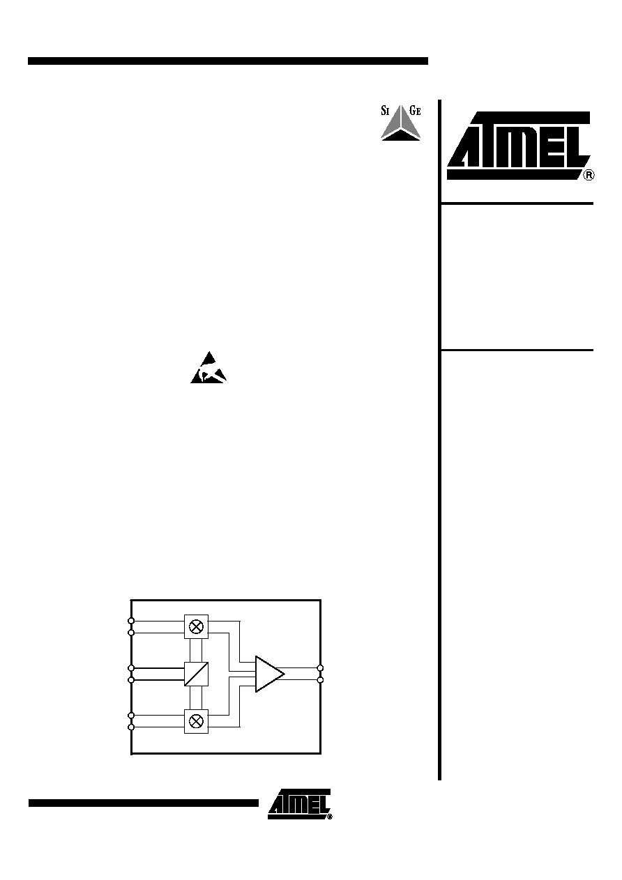
Figure 1. Block Diagram
13
12
16
1
4
5
8
9
BBQ-
BBQ+
BBI+
BBI-
LO+
LO-
RF+
RF-
90∞
0∞
700 MHz -
2700 MHz
Direct
Quadrature
Modulator
T0790
Preliminary

2
T0790 [Preliminary]
4555C≠SIGE≠11/03
Pin Configuration
Figure 2. Pinning SSOP16
BBQ-
VCC
GND
RF+
RF-
GND
VCC
BBI-
1
2
3
4
5
6
7
8
16
15
14
13
12
11
10
9
BBQ+
VCC
GND
LO+
LO-
GND
/SD
BBI+
Pin Description
Pin
Symbol
Function
1
BBQ+
Baseband Q-axis positive input
2
VCC
Supply voltage
3
GND
Ground
4
LO_IN+
Positive local oscillator input, nominal DC voltage is 2.0 V internally biased; input should be AC-coupled
5
LO_IN-
Negartive local oscillator input, nominal DC voltage is 2.0 V internally biased; input should be AC-coupled
6
GND
Ground
7
/SD
Shutdown control
8
BBI+
Baseband I-axis positive input
9
BBI-
Baseband I-axis negative input
10
VCC
Supply voltage
11
GND
Ground
12
RF_IN-
Negative RF output; nominal DC voltage is 2.4 Vinternally biased; input should be AC-coupled
13
RF_IN+
Positive RF output; nominal DC voltage is 2.4 V internally biased; input should be AC-coupled
14
GND
Ground
15
VCC
Supply voltage
16
BBQ-
Baseband Q-axis negative input
≠
Paddle
Device ground and heat sink, requires good thermal path; RF reference plane
Absolute Maximum Ratings
Stresses beyond those listed under "Absolute Maximum Ratings" may cause permanent damage to the device. This is a stress rating
only and functional operation of the device at these or any other conditions beyond those indicated in the operational sections of this
specification is not implied. Exposure to absolute maximum rating conditions for extended periods may affect device reliability.
Parameters
Symbols
Value
Unit
Supply voltage, no RF
applied
V
CC
5.5
V
LO input signals
LO_IN-, LO_IN+
+10.0
dBm
Input voltage
BBI+, BBI-, BBQ+, BBQ-
3
V
Operating case
temperature
T
C
-40 to +85
∞
C
Storage temperature
T
STG
-55 to +150
∞
C

3
T0790 [Preliminary]
4555C≠SIGE≠11/03
Thermal Resistance
Parameters
Symbols
Value
Unit
Junction ambient
R
thJA
35
K/W
Electrical Characteristics
Test conditions:
Unless otherwise noted, the following conditions apply to typical performance specification under static conditions:
V
CC
= 5 V, T
amb
= 25
∞
C; baseband inputs: 1.9 V DC bias, 200 kHz frequency, 300 mV
P-P
, 600 mV
P-P
differential drive, I/Q signals in
quadrature, LO = 1960 MHz; P
LO
= -5 dBm
No.
Parameters
Test Conditions
Pin
Symbol
Min.
Typ.
Max.
Unit
Type*
General Performance
Supply voltage
2, 10,
15
V
CC
4.75
5.0
5.25
V
A
Supply current
2, 10,
15
I
CC
73
82
mA
A
LO Input
LO drive
4, 5
P
LO
-8
-5
-2
dBm
D
LO frequency
4, 5
f
LO
700
2700
MHz
B
LO return loss
Matched to 50
4, 5
RL
LO
16
dB
C
Baseband Inputs
Baseband input
frequency range
-3 dB bandwidth,
baseband inputs,
terminated with 50
1, 8,
9, 16
f
BB
DC
500
MHz
D
Baseband input
resistance
Per pin
1, 8,
9, 16
R
BB
4.4
k
D
Baseband input
capacitance
Per pin
1, 8,
9, 16
C
BB
4
pF
D
Miscellaneous
Shutdown
attenuation
7
A
SD
60
dB
D
Shutdown pin
resistance
At 1 MHz
7
R
SD
11.9
k
D
Shutdown pin
capacitance
At 1 MHz
7
C
SD
5.2
pF
D
Shutdown input
thresholds
Shutdown disabled
(normal operation)
7
3.75
V
CC
V
D
Shutdown enabled
7
0
1.5
V
D
*) Type means: A = 100% tested, B = 100% correlation tested, C = Characterized on samples, D = Design parameter

4
T0790 [Preliminary]
4555C≠SIGE≠11/03
RF Electrical Characteristics (700 to 1000 MHz)
Test conditions:
Unless otherwise noted, the following conditions apply to typical performance specification under static conditions:
V
CC
= 5 V, T
amb
= 25
∞
C; baseband inputs: 1.9 V DC bias, 200 kHz frequency, 300 mV
P-P
, 600 mV
P-P
differential drive, I/Q signals in
quadrature, LO = 900 MHz; P
LO
= -5 dBm
No.
Parameters
Test Conditions
Pin
Symbol
Min.
Typ.
Max.
Unit
Type*
RF Output Port
RF frequency
12, 13
f
RF
700
1000
MHz
B
Output power
12, 13
P
RFout
-13.0
-10.5
-9.0
dBm
A
RF return loss
Matched to 50
12, 13
P
LORL
20
dB
D
1-dB output
compression point
12, 13
P1dB
3
4
dBm
A
LO-RF leakage
12, 13
P
LORF
-40
-34
dBm
D
Sideband
suppression
12, 13
A
SB
34
40
dB
D
IM3 suppression
Two tone baseband
input at 600 mV
P-P
differential per tone
12, 13
A
IM3
58
62
dB
D
Broadband noise
floor
12, 13
P
NOISE
-154
-148
dBm/
Hz
C
Quadrature phase
error
12, 13
-2
±0.5
+2
∞
B
I/Q amplitude balance
12, 13
-0.2
±0.5
+0.2
dB
B
*) Type means: A = 100% tested, B = 100% correlation tested, C = Characterized on samples, D = Design parameter
RF Electrical Characteristics (1700 to 2000 MHz)
Test conditions:
Unless otherwise noted, the following conditions apply to typical performance specification under static conditions:
V
CC
= 5 V, T
amb
= 25
∞
C; baseband inputs: 1.9 V DC bias, 200 kHz frequency, 300 mV
P-P
, 600 mV
P-P
differential drive, I/Q signals in
quadrature, LO = 1960 MHz; P
LO
= -5 dBm
No.
Parameters
Test Conditions
Pin
Symbol
Min.
Typ.
Max.
Unit
Type*
RF Output Port
RF frequency
12, 13
f
RF
1700
2000
MHz
B
Output power
12, 13
P
RFout
-15.0
-11.5
-10.0
dBm
A
RF return loss
Matched to 50
12, 13
P
LORL
16
dB
D
1-dB output
compression point
12, 13
P1dB
2
3
dBm
A
LO-RF leakage
12, 13
P
LORF
-40
-32
dBm
D
Sideband
suppression
12, 13
A
SB
34
40
dB
D
IM3 suppression
Two tone baseband
input at 600 mV
P-P
differential per tone
12, 13
A
IM3
58
62
dB
D
*) Type means: A = 100% tested, B = 100% correlation tested, C = Characterized on samples, D = Design parameter

5
T0790 [Preliminary]
4555C≠SIGE≠11/03
Broadband noise
floor
12, 13
P
NOISE
-155
-148
dBm/
Hz
C
Quadrature phase
error
12, 13
-2
±0.5
+2
∞
B
I/Q amplitude balance
12, 13
-0.2
±0.5
+0.2
dB
B
RF Electrical Characteristics (1700 to 2000 MHz) (Continued)
Test conditions:
Unless otherwise noted, the following conditions apply to typical performance specification under static conditions:
V
CC
= 5 V, T
amb
= 25
∞
C; baseband inputs: 1.9 V DC bias, 200 kHz frequency, 300 mV
P-P
, 600 mV
P-P
differential drive, I/Q signals in
quadrature, LO = 1960 MHz; P
LO
= -5 dBm
No.
Parameters
Test Conditions
Pin
Symbol
Min.
Typ.
Max.
Unit
Type*
*) Type means: A = 100% tested, B = 100% correlation tested, C = Characterized on samples, D = Design parameter
RF Electrical Characteristics (2300 to 2700 MHz)
Test conditions:
Unless otherwise noted, the following conditions apply to typical performance specification under static conditions:
V
CC
= 5 V, T
amb
= 25
∞
C; baseband inputs: 1.9 V DC bias, 200 kHz frequency, 300 mV
P-P
, 600 mV
P-P
differential drive, I/Q signals in
quadrature, LO = 2600 MHz; P
LO
= -5 dBm
No.
Parameters
Test Conditions
Pin
Symbol
Min.
Typ.
Max.
Unit
Type*
RF Output Port
RF frequency
12, 13
f
RF
2300
2700
MHz
B
Output power
12, 13
P
RFout
-18
-14.5
-13
dBm
A
RF return loss
Matched to 50
12, 13
P
LORL
15
dB
D
1-dB output
compression point
12, 13
P1dB
TBD
dBm
A
LO-RF leakage
12, 13
P
LORF
-40
-32
dBm
D
Sideband
suppression
12, 13
A
SB
34
40
dB
D
IM3 suppression
Two tone baseband
input at 600 mV
P-P
differential per tone
12, 13
A
IM3
TBD
dB
D
Broadband noise
floor
12, 13
P
NOISE
TBD
dBm/
Hz
C
Quadrature phase
error
12, 13
-2
±0.5
+2
∞
B
I/Q amplitude balance
12, 13
-0.2
±0.5
+0.2
dB
B
*) Type means: A = 100% tested, B = 100% correlation tested, C = Characterized on samples, D = Design parameter