 | –≠–ª–µ–∫—Ç—Ä–æ–Ω–Ω—ã–π –∫–æ–º–ø–æ–Ω–µ–Ω—Ç: T0790-6C | –°–∫–∞—á–∞—Ç—å:  PDF PDF  ZIP ZIP |

1
Features
∑
700 MHz to 2500 MHz Operating Frequency
∑
Very Low Noise Floor Performance
∑
Very Good Carrier and Sideband Suppression
∑
Supports Wideband Baseband Input
∑
Low LO Drive Requirements
∑
Power-down Mode
∑
No External IF Filter
∑
Supply Voltage 5 V
∑
Small SSOP16 Package
Applications
∑
Infrastructure Digital Communication Systems
∑
DCS/PCS/UMTS Transceivers
∑
ISM Band Transceivers
∑
GMSK, QPSK, QAM, 8PSK, SSB Modulators
Electrostatic sensitive device.
Observe precautions for handling.
Description
The T0790 is a direct quadrature modulator using Atmel's Silicon-Germanium (SiGe)
process. It features a frequency range from 700 up to 2500 MHz with excellent carrier
and sideband suppression and a low noise floor. The typical output power is -11 dBm
with an IM3 suppression greater than 60 dB.
The T0790 targets a wide range of communication applications including 3G wireless.
Figure 1. Block Diagram
13
12
16
1
4
5
8
9
BBQN
BBQP
BBIP
BBIN
LOP
LON
RFP
RFN
90∞
0∞
700 to 2500 MHz
Direct
Quadrature
Modulator
T0790
Preliminary
Rev. 4555A≠SIGE≠12/02

2
T0790
4555A≠SIGE≠12/02
Pin Configuration
Figure 2. Pinning SSOP16
BBON
VCC
GND
RFP
RFN
GND
VCC
BBIN
1
2
3
4
5
6
7
8
16
15
14
13
12
11
10
9
BBQP
VCC
GND
LOP
LON
GND
/SD
BBIP
Pin Description
Pin
Symbol
Function
1
BBQP
Q-channel baseband, positive input
2
VCC
+5 V power supply
3
GND
Ground
4
LOP
Local oscillator, positive input
5
LON
Local oscillator, negative input
6
GND
Ground
7
/SD
Shut-down control
8
BBIP
I-channel baseband, positive input
9
BBIN
I-channel baseband, negative input
10
VCC
+5 V power supply
11
GND
Ground
12
RFN
RF, negative output
13
RFP
RF, positive output
14
GND
Ground
15
VCC
+5 V power supply
16
BBQN
Q-channel baseband, negative input
3
T0790
4555A≠SIGE≠12/02
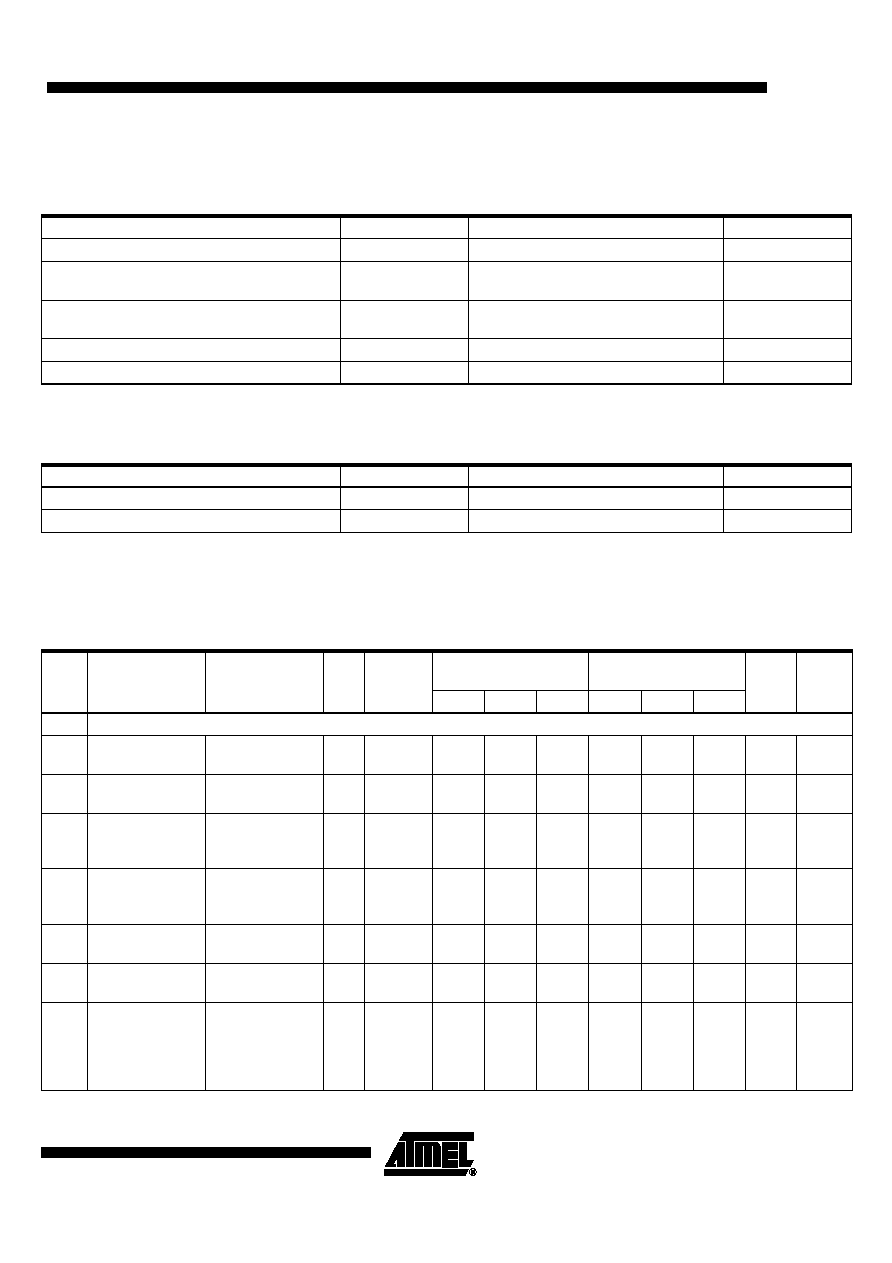
Absolute Maximum Ratings
All voltages are referred to GND.
Parameters
Symbols
Value
Unit
Supply voltage
V
CC
5.5
V
LO, RF input
LOP, LON, RFP,
RFN
10
dBm
Input voltage
BBIP, BBIN,
BBQP, BBQN
3
V
Operating temperature
T
OP
-40 to +85
∞
C
Storage temperature
T
stg
-65 to +150
∞
C
Thermal Resistance
Parameters
Symbols
Value
Unit
Junction ambient
R
thJA
TBD
K/W
Junction case
R
thJC
46
∞
C/W
Electrical Characteristics
Test conditions: V
CC
= +5 V, T
amb
= +25
∞
C, baseband inputs: 1.9 V DC bias, 200 kHz frequency, 300 mV
p-p
,
600 mV
p-p
differential drive, I/Q signals in quadrature, LO input: -5 dBm at 1960 MHz
No.
Parameters
Test Conditions
Pin Symbols
700 to 1000 MHz
Operation
1700 to 2500 MHz
Operation
Unit
Type*
Min.
Typ.
Max.
Min.
Typ.
Max.
1
RF Output
1.1
Frequency range
12,
13
f
700
1000
1700
2500
MHz
B
1.2
Output power
12,
13
P
RF out
-13.0
-10.5
-9.0
-15.0
-11.5
-10
dBm
A
1.3
RF port return
loss
Matched to 50
W
(refer to
schematics)
12,
13
RL
20
16
dB
D
1.4
1dB-output
compression
point
Compression
point
12,
13
P1dB
3
4
2
3
dBm
A
1.5
LO leakage
12,
13
A
LO
-40
-34
-40
-32
dBm
D
1.6
Sideband
suppression
12,
13
A
SB
34
40
34
40
dB
D
1.7
IM3 suppression
Two-tone
baseband input at
600 mV
p-p
differential per
tone
12,
13
A
IM3
58
62
58
65
dB
D
*) Type means: A = 100% tested, B = 100% correlation tested, C = Characterized on samples, D = Design parameter.

4
T0790
4555A≠SIGE≠12/02
1.8
Broadband noise
floor
Baseband inputs
tied to 1.9 V
DC
,
-20 MHz offset
from carrier
12,
13
P
noise
-154
-148
-155
-148
dBm/
Hz
C
1.9
Quadrature
phase error
12,
13
-2
±0.5
+2
-2
±0.5
+2
∞
C
B
1.10 I/Q amplitude
balance
12,
13
-0.2
±0.5
+0.2
-0.2
±0.5
+0.2
dB
B
2
Modulation Input
2.1
Baseband
frequency input
-3dB bandwidth,
baseband inputs
terminated in
50
W
1, 8,
9, 16
f
BB
DC
500
DC
500
MHz
D
2.2
Baseband input
resistance
Per pin
1, 8,
9, 16
R
BB
4.4
4.4
k
W
D
2.3
Baseband input
capacitance
Per pin
1, 8,
9, 16
C
BB
0.5
0.5
pF
D
3
LO Input
3.1
LO frequency
4, 5
f
LO
700
2500
700
2500
MHz
B
3.2
LO drive level
4, 5
P
LO
-8
-5
-2
-8
-5
-2
dBm
D
3.3
LO port return
loss
Matched to 50
W
(refer to
schematic)
4, 5
RL
LO
16
16
dB
C
4
Miscellaneous
4.1
Shut-down
attenuation
7
A
SD
60
60
dB
D
4.2
Shut-down pin
resistance
at 1 MHz
7
R
SD
11.9
11.9
k
W
D
4.3
Shut-down pin
capacitance
at 1 MHz
7
C
SD
5.2
5.2
pF
D
4.4
Shut-down input
thresholds
Shut-down
disabled (normal
operation)
7
3.75
V
CC
3.75
V
CC
V
D
Shut-down
enable
7
0
1.5
0
1.5
V
D
Electrical Characteristics (Continued)
Test conditions: V
CC
= +5 V, T
amb
= +25
∞
C, baseband inputs: 1.9 V DC bias, 200 kHz frequency, 300 mV
p-p
,
600 mV
p-p
differential drive, I/Q signals in quadrature, LO input: -5 dBm at 1960 MHz
No.
Parameters
Test Conditions
Pin Symbols
700 to 1000 MHz
Operation
1700 to 2500 MHz
Operation
Unit
Type*
Min.
Typ.
Max.
Min.
Typ.
Max.
*) Type means: A = 100% tested, B = 100% correlation tested, C = Characterized on samples, D = Design parameter.

5
T0790
4555A≠SIGE≠12/02
4.5
Shut-down
settling time
7
16
16
ns
4.6
Supply voltage
2,
10,
15
V
CC
4.75
5
5.25
4.75
5
5.25
V
A
4.7
Supply current
2,
10,
15
73
82
73
82
mA
A
Electrical Characteristics (Continued)
Test conditions: V
CC
= +5 V, T
amb
= +25
∞
C, baseband inputs: 1.9 V DC bias, 200 kHz frequency, 300 mV
p-p
,
600 mV
p-p
differential drive, I/Q signals in quadrature, LO input: -5 dBm at 1960 MHz
No.
Parameters
Test Conditions
Pin Symbols
700 to 1000 MHz
Operation
1700 to 2500 MHz
Operation
Unit
Type*
Min.
Typ.
Max.
Min.
Typ.
Max.
*) Type means: A = 100% tested, B = 100% correlation tested, C = Characterized on samples, D = Design parameter.