 | –≠–ª–µ–∫—Ç—Ä–æ–Ω–Ω—ã–π –∫–æ–º–ø–æ–Ω–µ–Ω—Ç: T0797 | –°–∫–∞—á–∞—Ç—å:  PDF PDF  ZIP ZIP |

1 (10)
Preliminary Information
Features
∑
Gain control in 20-dB steps
∑
Very low I/Q amplitude and phase errors
∑
High input P1dB
∑
Buffered IF OUT available through baseband output
Applications
∑
Infrastructure digital communication systems
∑
GSM/cellular transceivers
∑
ISM band transceivers
Electrostatic sensitive device.
Observe precautions for handling.
Description
The T0797 is a multi-purpose demodulator RFIC. The silicon monolithic integrated cir-
cuit is a designed in Atmels advanced SiGe technology. This demodulator is capable
of both quadrature demodulation or direct IF output. Features include switchable gain
control on a frequency range from 65 MHz to 300 MHz. The device performs a very
low amplitude as well as phase error and allows high input P1dB. The T0797 targets a
variety of system applications for communications including 3G wireless.
Block Diagram
Figure 1.
IFP
IFN
GC1
GC2
BBIP
BBIN
BBQP
BBQN
LOP
LON
1
2
16
15
12
13
4
5
8
9
65 - 300 MHz
SiGe IF
Receiver /
Demodulator
T0797
Rev. A2, 03-Dec-01
2 (10)
Preliminary Information
T0797
Rev. A2, 03-Dec-01
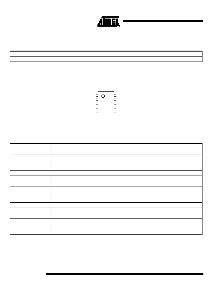
Pin Configuration
Figure 2.
Ordering Information
Extended Type Number
Package
Remarks
T0797
TSSOP16
BBQP
BBQN
VCC
LOP
LON
GND
VCC
IFN
1
2
3
4
5
6
7
8
16
15
14
13
12
11
10
9
BBIN
BBIP
VCC
GC2
GC1
GND
VCC
IFP
Pin Description
Pin
Symbol
Function
1
BBIN
Baseband I-axis negative output
2
BBIP
Baseband I-axis positive output
3
VCC
5 V power supply
4
GC2
Gain control input, stage 2
5
GC1
Gain control input, stage 1
6
GND
Ground
7
VCC
5 V power supply
8
IFP
IF positive input
9
IFN
IF negative input
10
VCC
5 V power supply
11
GND
Ground
12
LON
Local oscillator, negative input
13
LOP
Local oscillator, positive input
14
VCC
5 V power supply
15
BBQN
Baseband Q-axis negative output
16
BBQP
Baseband Q-axis positive output

3 (10)
Preliminary Information
T0797
Rev. A2, 03-Dec-01
Note:
The part may not survive all maximums applied simultaneously
Absolute Maximum Ratings
All voltages are referred to GND.
Parameter
Symbol
Value
Unit
Supply voltage
V
CC
5.5
V
LO input
LOP, LON
10
dBm
IF input
IFN, IFP
10
V
Operating temperature
T
OP
-40 to +85
∞C
Storage temperature
T
stg
-65 to +150
∞C
Thermal Resistance
Parameter
Symbol
Value
Unit
Junction ambient
R
thJA
tbd
K/W
Electrical Characteristics
Test conditions: V
CC
= 5 V, T
amb
= 25∞C, LO input: 0 dBm@200 MHz
IF input: @200.1 MHz, GC1 = 0, GC2 = 0; 0 dBm
IF input: @200.1 MHz, GC1 = 1, GC2 = 0; -20 dBm
IF input: @200.1 MHz, GC1 = 1, GC2 = 1; -40 dBm
No.
Parameters
Test Conditions
Pin
Symbol
Min.
Typ.
Max.
Unit
Type*
1
IF input (I/Q mixing to baseband)
1.1
Frequency range
8, 9
f
65
120 -
220
300
MHz
B
1.2
Return loss
8, 9
RL
20
dB
D
1.3
Gain
Gain set = high; GC1
= GC2 = 1
8, 9
G
35
dB
A
1.4
Input P1dB
8, 9
P1dB
≠30
dBm
C
1.5
Input IP3
8, 9
IIP3
≠20
dBm
B
1.6
Noise figure
8, 9
NF
6
dB
D
1.7
Gain
Gain set = high; GC1
= 1; GC2 = 0
8, 9
G
15
dB
A
1.8
Input P1dB
8, 9
P1dB
≠10
dBm
C
1.9
Input IP3
8, 9
IIP3
0
dBm
B
1.10
Noise figure
8, 9
NF
≠3
10
dB
D
1.11
Gain
Gain set = high; GC1
= GC2 = 0
8, 9
G
≠5
dB
A
1.12
Input P1dB
8, 9
P1dB
10
dBm
C
1.13
Input IP3
8, 9
IIP3
20
dBm
B
1.14
Noise figure
8, 9
NF
30
dB
D
*) Type means: A = 100% tested, B = 100% correlation tested, C = Characterized on samples, D = Design parameter

4 (10)
Preliminary Information
T0797
Rev. A2, 03-Dec-01
2
Stuck Mixer (DC to LO port ≠ gain-controlled amplifier)
2.1
Frequency range
8, 9
f
65
120 -
220
300
MHz
B
2.2
Return loss
8, 9
RL
20
dB
D
2.3
Gain
Gain set = high;
GC1 = GC2 = 1
8, 9
G
40
dB
A
2.4
Input P1dB
8, 9
P1dB
≠26
dBm
C
2.5
Input IP3
8, 9
IIP3
≠16
dBm
B
2.6
Noise figure
8, 9
NF
6
dB
D
2.7
Gain
Gain set = high;
GC1 = 1; GC2 = 0
8, 9
G
20
dB
A
2.8
Input P1dB
8, 9
P1dB
≠6
dBm
C
2.9
Input IP3
8, 9
IIP3
4
dBm
B
2.10
Noise figure
8, 9
NF
9
dB
D
2.11
Gain
Gain set = high;
GC1 = GC2 = 0
8, 9
G
0
dB
A
2.12
Input P1dB
8, 9
P1dB
14
dBm
C
2.13
Input IP3
8, 9
IIP3
24
dBm
B
2.14
Noise figure
8, 9
NF
30
dB
D
3
I/Q Output
3.1
I/Q output frequency
range
1, 2,
15, 16
f
I/Q
DC
500
MHz
D
3.2
I/Q output amplitude
error
1, 2,
15, 16
≠0.2
+0.2
dB
A
3.3
I/Q phase error
1, 2,
15, 16
≠2
+2
deg
A
3.4
I/Q output common
mode voltage
1, 2,
15, 16
2.5
V
A
3.5
I/Q output differential
offset voltage
1, 2,
15, 16
V
offset
10
mV
A
4
LO input
4.1
LO input level
12, 13
P
LO
≠3
0
+3
dBm
D
4.2
Return loss
12, 13
RL
LO
20
dB
D
5
Miscellaneous
5.1
Supply voltage
3, 7,
10, 14
V
CC
4.75
5
5.25
V
A
5.2
Supply current
3, 7,
10, 14
I
CC
180
mA
A
Electrical Characteristics
Test conditions: V
CC
= 5 V, T
amb
= 25∞C, LO input: 0 dBm@200 MHz
IF input: @200.1 MHz, GC1 = 0, GC2 = 0; 0 dBm
IF input: @200.1 MHz, GC1 = 1, GC2 = 0; -20 dBm
IF input: @200.1 MHz, GC1 = 1, GC2 = 1; -40 dBm
No.
Parameters
Test Conditions
Pin
Symbol
Min.
Typ.
Max.
Unit
Type*
*) Type means: A = 100% tested, B = 100% correlation tested, C = Characterized on samples, D = Design parameter

5 (10)
Preliminary Information
T0797
Rev. A2, 03-Dec-01
Typical Device
Performance
Figure 3.
Gain vs. pin high-gain state (11
)
Figure 4.
Gain vs. pin low-gain state (00)
Figure 5.
Gain vs. pin medium-gain state (10)
30
31
32
33
34
35
-40
-38
-36
-34
-32
-30
-28
-26
Pin (dBm )
G
a
in (dB
)
- 8
- 7
- 6
- 5
- 4
- 3
0
5
1 0
15
Pin ( d Bm )
G
a
in
(
d
B)
11
12
13
14
15
16
-20
-18
-16
-14
-12
-10
-8
-6
Pin (dBm )
G
a
in (dB
)