 | –≠–ª–µ–∫—Ç—Ä–æ–Ω–Ω—ã–π –∫–æ–º–ø–æ–Ω–µ–Ω—Ç: T0815 | –°–∫–∞—á–∞—Ç—å:  PDF PDF  ZIP ZIP |

1
Features
∑
Current-controlled Output Current Source, 3 Input Channels
∑
Low Power Consumption
∑
Output Current per Channel to 250 mA
∑
Total Output Current to 300 mA
∑
Rise Time 1.0 ns, Fall Time 1.1 ns
∑
On-chip RF Oscillator
∑
Control of Frequency and Swing by Use of 2 External Resistors
∑
Oscillator Frequency Range from 200 MHz to 500 MHz
∑
Oscillator Swing to 100 mA
∑
Fast Settling APC Amplifier
∑
Single 5 V Power Supply
∑
Common Enable, Disable Input
∑
TTL/CMOS Control Signals
∑
Small SSO16 Package
Applications
∑
CD-RW Drives
∑
Writable Optical Drives
Description
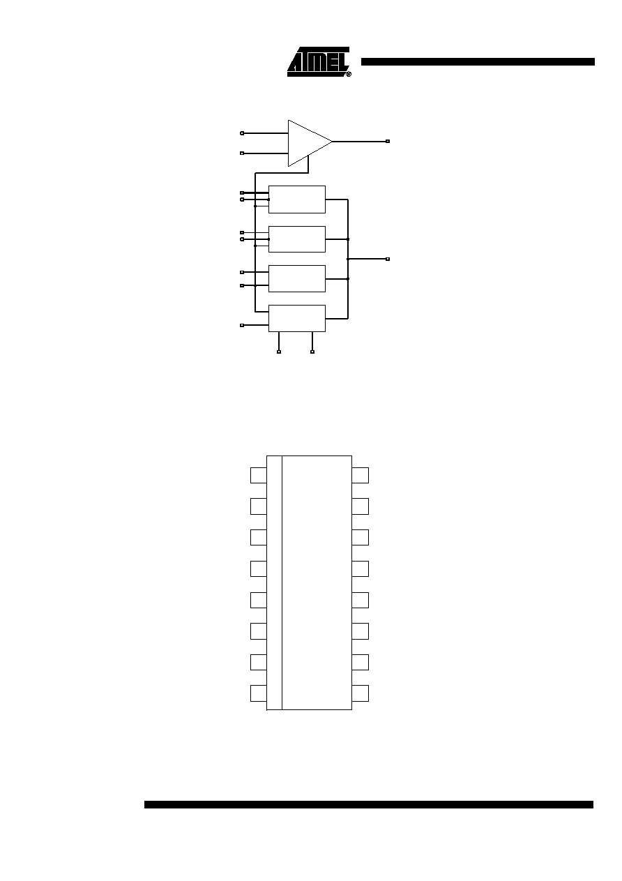
The T0815 is a laser diode driver for the operation of a grounded laser diode for CD-
RW drives. It includes three channels for three different optical power levels which are
controlled by a separate IC. The read channel generates a continuous output level
whereas the channels 2 and 3 are provided as write channels with very fast switching
speeds. Write current pulses are enabled when a `low' signal is applied to the NE pins.
All channels are summed together at the IOUT pin. Each channel can contribute up to
250 mA to the total output current of up to 300 mA. A total gain of 400 is provided
between each reference current input and the output. Although the reference inputs
are current inputs; voltage control is possible by using external resistors.
An on-chip RF oscillator is provided to reduce laser mode hopping noise during read
mode. Frequency and swing can be set by two external resistors. Oscillation is
enabled by a `high' at the ENOSC pin. Complete output current and oscillator switch-
off is achieved by a `low' at the ENABLE input.
The T0815 also includes a fast settling APC (Adaptive Power Control) transimpedance
amplifier. It is provided to interface between the front end monitor photo diode and the
ALPC (Adaptive Laser Diode Power Controller) circuit.
3-Channel Laser
Driver with RF
Oscillator and
APC Amplifier
T0815
Rev. 4504B≠DVD≠06/02
2
T0815
4504B≠DVD≠06/02
Figure 1. Block Diagram
Pin Configuration
Figure 2. Pinning SSO16
APC
Channel 3
Channel 2
I3
NE3
I2
NE2
Read channel
RF oscillator
IR
ENOSC
ENABLE
IOUT
VREF
PDIN
VOUT
RF
RS
1
2
3
4
5
6
7
8
16
15
14
13
12
11
10
9
IR
RF
I2
I3
NE2
NE3
VOUT
VREF
IOUT
GND
RS
ENABLE
ENOSC
VCC2
PDIN
VCC1
T0815
3
T0815
4504B≠DVD≠06/02
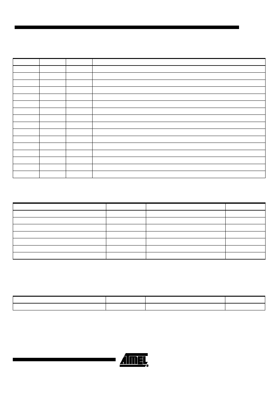
Pin Description
Pin
Symbol
Type
Function
1
VOUT
analog
APC amplifier output
2
VREF
analog
Reference voltage input
3
IR
analog
Input current, bias voltage approximately GND
4
RF
analog
External resistor to GND sets oscillator frequency
5
I2
analog
Input current, bias voltage approximately GND
6
I3
analog
Inp. current, bias voltage approximately GND
7
NE2
digital
Digital control of channel 2 (low active)
8
NE3
digital
Digital control of channel 3 (low active)
9
VCC2
supply
+ 5 V power supply for IOUT
10
ENOSC
digital
Enables RF oscillator (high active)
11
ENABLE
digital
Enables output current (high active)
12
RS
analog
External resistor to GND sets oscillator swing
13
GND
supply
Ground
14
IOUT
analog
Output current source for laser diode
15
VCC1
supply
+ 5 V power supply for IOUT and circuit
16
PDIN
analog
Photo diode input
Absolute Maximum Ratings
Parameters
Symbol
Value
Unit
Supply voltage
V
CC
-0.5 to +6.0
V
Input voltage at IR, I2, I3
V
IN1
-0.5 to + 2.0
V
Input voltage at NE2, NE3, ENOSC
V
IN2
-0.5 to V
CC
+ 0.5
V
Output voltage
V
OUT
-0.5 to V
CC
≠1
V
Power dissipation
P
Max
0.7
(1)
to 1
(2)
W
Junction temperature
T
J
150
∞
C
Storage temperature range
T
Stg
-65 to +125
∞
C
Notes: 1. R
thJA
£
115 K/W, T
amb
= 70∞C
2.
R
thJA
£
115 K/W, T
amb
= 25∞C
Thermal Resistance
Parameters
Symbol
Value
Unit
Junction ambient
R
thJA
115
(1)
K/W
Note:
1. Measured with multi-layer test board (JEDEC standard)
4
T0815
4504B≠DVD≠06/02
Operating Range
Parameters
Symbol
Value
Unit
Supply voltage range
V
CC
4.5 to 5.5
V
Input current
I
IR
/I
I2
/I
I3
< 1
mA
External resistor to GND to set oscillator
frequency
RF
> 3
k
W
External resistor to GND to set oscillator swing
RS
> 1
k
W
Operating temperature range
T
amb
0 to +70
∞C
Electrical Characteristics: General
V
CC
= 5 V, T
amb
=25∞C, ENABLE = High, NE2 = NE3 = High, ENOSC = Low, unless otherwise specified
No.
Parameters
Test Conditions
Pin
Symbol
Min.
Typ.
Max.
Unit
Type*
1
Power Supply
1.1
Supply current, power
down
ENABLE = Low,
NE2 = NE3 = Low
9, 15
ICC
PD
0.3
mA
A
1.2
Supply current, read
mode, Oscillator
disabled
I
IR
= I
I2
= I
I3
= 125 µA
9, 15
ICC
R1
90
mA
A
1.3
Supply current, read
mode, Oscillator
enabled
I
IR
= I
I2
= I
I3
= 125 µA,
ENOSC = High,
RS = 7.5 k
W
,
RF = 7.5 k
W
9, 15
ICC
R2
95
mA
A
1.4
Supply current, write
mode
I
IR
= I
I2
= I
I3
= 125 µA,
NE2 = NE3 = Low
9, 15
ICC
W
190
mA
A
1.5
Supply current, input
off
I
IR
= I
I2
= I
I3
= 0 µA
9, 15
ICC
off
17
mA
A
2
Digital Inputs
2.1
NE2/NE3 low voltage
7, 8
VNE
LO
1.3
V
A
2.2
NE2/NE3 high
voltage
7, 8
VNE
HI
2.0
V
A
2.3
ENABLE low voltage
11
VEN
LO
0.5
V
A
2.4
ENABLE high voltage
11
VEN
HI
3.0
V
A
2.5
ENOSC low voltage
10
VEO
LO
0.5
V
A
2.6
ENOSC high voltage
10
VEO
HI
3.0
V
A
3
Current at Digital Inputs
3.1
NE2/NE3 low current
NE = 0 V
7, 8
INE
LO
-300
µA
A
3.2
NE2/NE3 high current
NE = 5 V
7, 8
INE
HI
800
µA
A
3.3
ENABLE low current
ENABLE = 0 V
11
IEN
LO
-150
µA
A
3.4
ENABLE high current
ENABLE = 5 V
11
IEN
HI
100
µA
A
3.5
ENOSC low current
ENOSC = 0 V
10
IEO
LO
-100
µA
A
3.6
ENOSC high current
ENOSC = 5 V
10
IEO
HI
800
µA
A
*) Type means: A =100% tested, B = 100% correlation tested, C = Characterized on samples, D = Design parameter

5
T0815
4504B≠DVD≠06/02
Electrical Characteristics: Laser Amplifier
V
CC
= 5 V, T
amb
= 25∞C, ENABLE = High, unless otherwise specified
No.
Parameters
Test Conditions
Pin
Symbol
Min.
Typ.
Max.
Unit
Type*
4
Laser Amplifier
4.1
Total output current
Output is sourcing
14
I
OUT
300
350
mA
A
4.2
Output current per
channel
Output is sourcing
14
I
OUT
250
mA
A
4.3
I
OUT
series resistance
Total R
OUT
to V
CC
rail
14
R
OUT
6
W
A
4.4
Best fit current gain
Any channel
(1)
14
GAIN
355
400
485
mA/mA
A
4.5
Best fit current offset
Any channel
(1)
14
IOS
-8
+4
mA
A
4.6
Output current
linearity
Any channel
(1)
14
ILIN
-3
+3
%
A
4.7
I
IN
input impedance
R
IN
is to GND
3, 5, 6
R
IN
1200
2000
2500
W
A
4.8
NE threshold
Temperature
stabilized
7, 8
VTH
1.68
V
B
4.9
Output off current 1
ENABLE = Low
14
IOFF
1
1
mA
A
4.10
Output off current 2
NE2 = NE3 = High,
I
IR
= 0,
I
I2
= I
I3
= 125 µA
14
IOFF
2
1
mA
A
4.11
Output off current 3
NE2 = NE3 = Low,
I
IR
= I
I2
= I
I3
= 0 µA
14
IOFF
3
5
mA
A
4.12
I
OUT
supply sensitivity,
read mode
I
OUT
= 40 mA,
V
CC
= 5 V
±
10%,
read only
14
VSE
R
-4
1
%/V
A
4.13
I
OUT
supply sensitivity,
write mode
I
OUT
= 80 mA, 40 mA
read + 40 mA write,
V
CC
= 5 V
±
10%
14
VSE
W
-6
0
%/V
A
4.14
I
OUT
current output
noise
I
OUT
= 40 mA,
ENOSC = Low
14
INO
O
3
nA/
rt-Hz
C
4.15
I
OUT
temperature
sensitivity,
read mode
I
OUT
= 40 mA,
read only
14
TSE
R
-400
ppm/
∞
C
C
4.16
IOUT temperature
sensitivity, write mode
I
OUT
= 80 mA, 40 mA
read + 40 mA write
14
TSE
W
-400
ppm/∞C
C
*) Type means: A =100% tested, B = 100% correlation tested, C = Characterized on samples, D = Design parameter
Note:
1. Linearity of the amplifier is calculated using a best fit method at three operating points of I
OUT
at 20 mA, 40 mA,
and 60 mA. I
OUT
= (I
IN
¥
GAIN) + I
OS