
T2801
Preliminary Information
Rev. A9, 11-Dec-01
1 (27)
DECT Single-Chip Transceiver
Description
The T2801 is an RF IC for low-power DECT appli-
cations. The HP-VFQFP-N48-packaged IC is a complete
transceiver including image rejection mixer, IF amplifier,
FM demodulator, baseband filter, RSSI, TX preamplifier,
power-ramping generator for power amplifiers, inte-
grated synthesizer, fully integrated VCO, TX filter and
modulation compensation circuit for advanced closed-
loop modulation concept. No mechanical tuning is
necessary in production.
Electrostatic sensitive device.
Observe precautions for handling.
Features
D Supply-voltage range 3 V to 4.6 V (unregulated)
D Auxiliary-voltage regulator on-chip
D Low current consumption
D Few low cost external components
D No mechanical tuning required
D Non-blindslot and blindslot operation
D Unlimited multislot operation with advanced closed-
loop modulation
D Supports multiple reference clocks (10.368 MHz/
13.824 MHz/ 20.736 MHz)
D TX preamplifier with 0 dBm output power at 1.9 GHz
and ramp-signal generator for SiGe power amplifier
Block Diagram
TANK
PC
RC
GF
MCC
CP
VCO
f
: n
f
: n
CTRL
LOGIC
PD
TX / RX
SWITCH
IR MIXER
IF AMP 1
IF AMP 2
DEMOD
BB FILTER
3-WIRE
BUS
DEMOD DAC
RSSI
TX DRIVER
CLOCK
DATA
ENABLE
RX_ON
TX_ON
PU_RX/TX
PU_PLL
TX_DATA
RSSI
BB_OUT
CF
DEMOD
IF_TANK
IF_IN
MIXER
OUT
RF_IN
TX_OUT
VS_VCO
CP
LD
REF_CLK
VTUNE
VREG
VS_REG
REG_CTRL
VREG_VCO
VCO
REG
RAMP
GEN
RAMP_OUT
RAMP_SET
AUX
REG
PU_VCO
PU_REG
GND_VCO
D/A
I_CPSW
Figure 1. Block diagram
Ordering Information
Extended Type Number
Package
Remarks
T2801-PLH
HP-VFQFP-N48
Taped and reeled

T2801
Rev. A9, 11-Dec-01
Preliminary Information
2 (27)
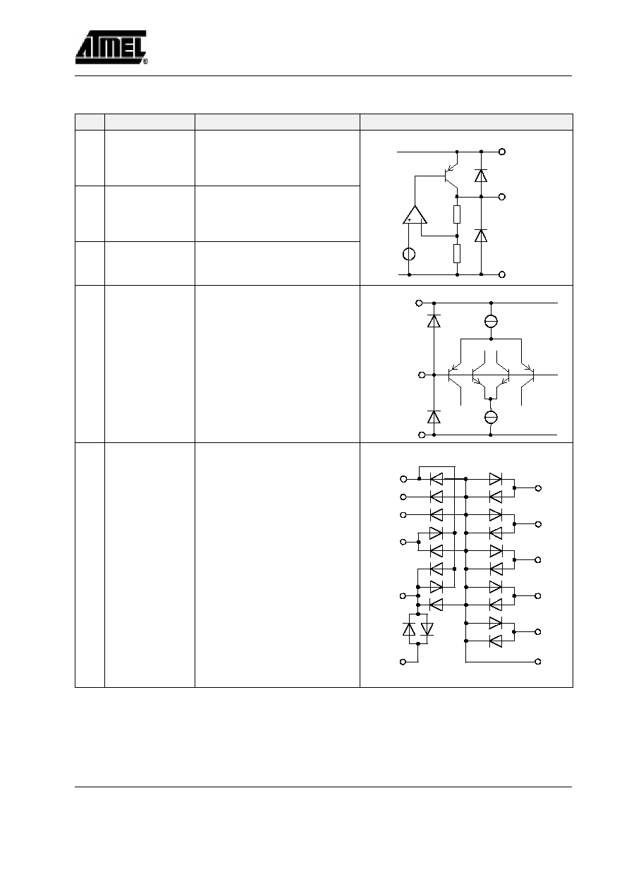
Functional Block Description
Name
Description
AUX REG
Auxiliary voltage regulator
BBF
Baseband filter
CP
Charge pump
DAC
D/A converter for demodulator tuning
DEMOD
Demodulator
GF
Gaussian filter for transmit data
IF AMP1
1st intermediate frequency amplifier
IF AMP2
2nd intermediate frequency amplifier
IR MIXER
Image rejection mixer
MCC
Modulation compensation circuit
Name
Description
PC
Programmable counter
PD
Phase detector
RAMP GEN
Ramp-signal generator
RC
Reference counter
RSSI
Received signal-strength indicator
TX DRIVER
Buffer amplifier for TX_OUT
TX/RX
SWITCH
Switches VCO signal to IR MIXER
resp. TX DRIVER
VCO
Voltage-controlled oscillator
VCO REG
Voltage regulator for VCO
Pinning
CLOCK
DATA
ENABLE
REF_CLK
LD
PU_REG
VS_PLL
VREG
REG_CTRL
VS_REG
GND_CP
VS_CP
RAMP_OUT
IF_IN2
IF_IN1
VS_IF
TX_OUT
GND3
RF_IN2
RF_IN1
GND2
IF_TANK2
IF_TANK1
RSSI
1
2
3
4
5
6
7
8
9
10
11
12
13
14
15
16
17
18
19
20
21
22
23
24
36
35
34
33
32
31
30
29
28
27
26
25
48
47
46
45
44
43
42
41
40
39
38
37
T2801
RX_ON
TX_ON
MIXER_OUT1
PU_VCO
TX_DA
T
A
VS_MIXER
GND_PLL
PU_RX/TX
PU_PULL
I_CPSW
RAMP_SET
MIXER_OUT2
CP
GND_VCO
VS_VCO
GND1
VTUNE
VREG_VCO
BB_OUT
DAC_DEC
BB_CF
REG_DEC
DEMOD_T
ANK2
DEMOD_T
ANK1
Figure 2. Pinning

T2801
Preliminary Information
Rev. A9, 11-Dec-01
3 (27)
Pin Description
Pin
Symbol
Function
Configuration
1
CLOCK
3-wire-bus: Clock input
VS_PLL
7
2
DATA
3-wire-bus: Data input
CLOCK
DATA
ENABLE
1 2 3
3
ENABLE
3-wire-bus: Enable input
ENABLE
1,2,3
5k
5k
GND_PLL
43
4
REF_CLK
Reference-frequency input
VS_PLL
7
REF_CLK
4
10k
GND_PLL
43
10k
5
LD
Lock-detect output
GND_PLL
43
100
LD
5
6
PU_REG
Power-up input for aux. voltage
regulator
PU_REG
6
25k
25k
GND_PLL
43

T2801
Rev. A9, 11-Dec-01
Preliminary Information
4 (27)
Pin Description (continued)
Pin
Symbol
Function
Configuration
7
VS_PLL
PLL supply voltage
GND_PLL
43
GND2
28
GND1
18
GND3
31
GND_CP
11
GND_VCO
16
VS_MIXER
42
VS_IF
33
VS_VCO
14
VS_CP
12
VS_REG
10
VS_PLL
7
8
VREG
Aux. voltage-regulator output
REG_CTRL
9
VS_REG
10
9
REG_CTRL
Aux. voltage-regulator control
output
VREG
8
10
VS_REG
Aux. voltage-regulator supply
voltage
GND_PLL
43
11
GND_CP
Charge-pump ground
VS_CP
12
12
VS_CP
Charge-pump supply voltage
CP
13
13
CP
Charge-pump output
GND_CP
11
T2801
Preliminary Information
Rev. A9, 11-Dec-01
5 (27)
Pin Description (continued)
Pin
Symbol
Function
Configuration
14
VS_VCO
VCO voltage-regulator supply
voltage
VS_VCO
14
VREG VCO
15
VREG_VCO
VCO voltage-regulator control
output
VREG_VCO
15
16
GND_VCO
VCO ground
GND_VCO
16
17
VTUNE
VCO tuning voltage input
VTUNE
17
GND_VCO
16
VREG_VCO
15
18
GND1
Ground
GND_PLL
43
GND2
28
GND1
18
GND3
31
GND_CP
11
GND_VCO
16
VS_MIXER
42
VS_IF
33
VS_VCO
14
VS_CP
12
VS_REG
10
VS_PLL
7