T4227
Preliminary Information
Rev. A3, 20-Mar-01
1 (14)
Time-Code Receiver
Description
The T4227 is a bipolar integrated straight-through receiver circuit in the frequency range of 40 kHz to 120 kHz.
The device is designed for radio-controlled clock applications with very high sensitivity and low power consumption.
Features
D Low power consumption
D Very high sensitivity (0.4 mV)
D High selectivity by using crystal filter
D Power-down mode available
D Only a few external components necessary
D Complementary output stages
D AGC hold mode
D Wide frequency range (40 kHz to 120 kHz)
D Low battery voltage applications (1.1 V to 3.6 V)
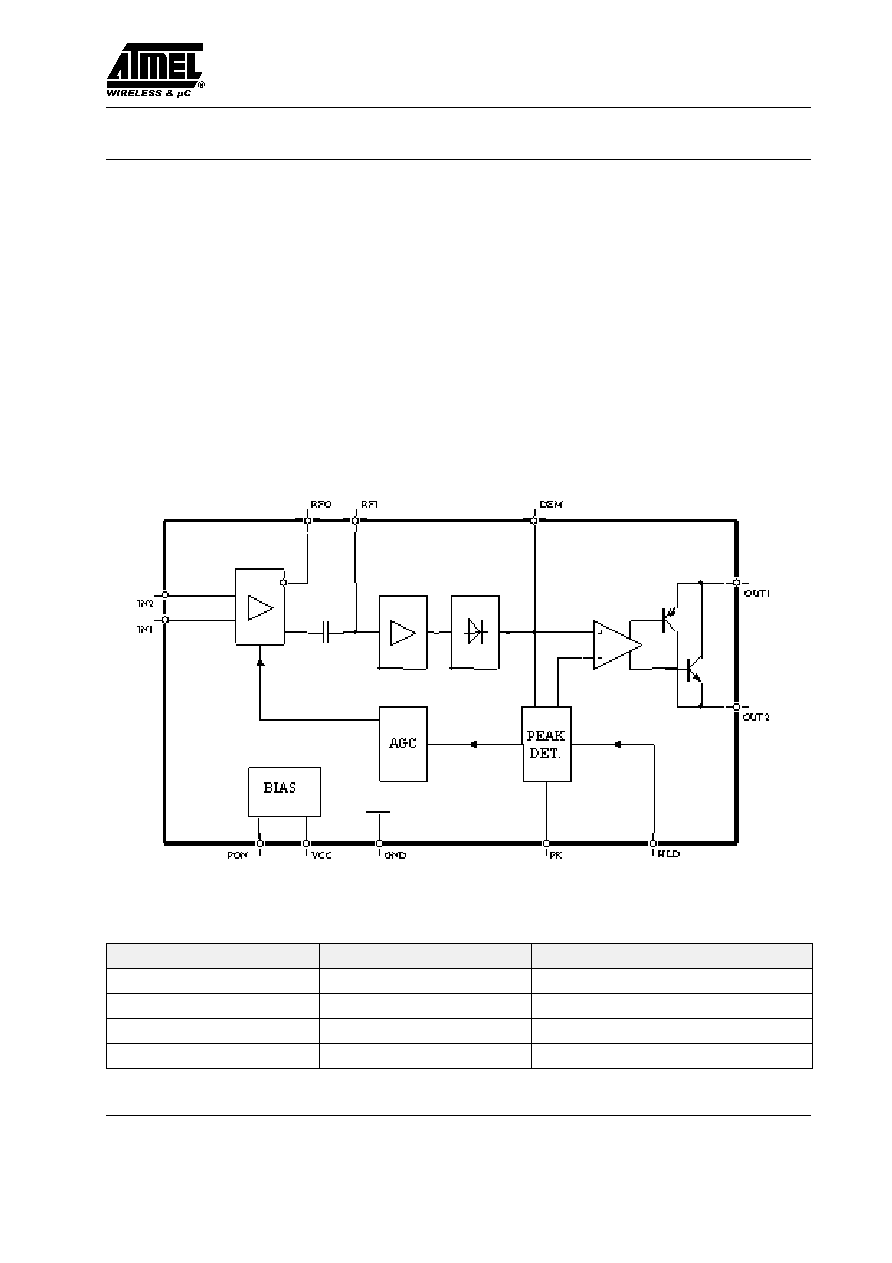
Block Diagram
Figure 1. Block diagram
Ordering Information
Extended Type Number
Package
Remarks
T4227-DDT
No
Die in trace
T4227-FB
SSO16
T4227-FBG3
SSO16
Taped and reeled
T4227-DBQ
No
CSP Chip Scale Package
T4227
Rev. A3, 20-Mar-01
Preliminary Information
2 (14)
Absolute Maximum Ratings
Parameter
Symbol
Value
Unit
Supply voltage
V
CC
5.5
V
Ambient temperature range
T
amb
�40 to +85
_C
Storage temperature range
R
stg
�55 to +150
_C
Junction temperature
T
j
125
_C
Electrostatic handling (MIL Standard 883 D HBM)
�
V
ESD
2000
V
PAD Coordinates
The T4227 is available as die for "chip-on-board" mounting and in SSO16 package.
DIE size:
1.65 x 1.44 mm
PAD size:
100 x 100
�
m (contact window 88 x 88
�
m)
Thickness:
300
�
m
�
10
�
m
Symbol
Function
x�axis (
mm)
y�axis (
mm)
Pad # (dice)
Pin # (SSO16*)
RFI
RF-input (from crystal)
130
1141
1
2
GND
Ground
130
934
2
3
RFO
RF-output (to crystal)
130
727
3
4
Vcc
Supply voltage
130
520
4
5
IN2
Antenna input 2
130
313
5
6
IN1
Antenna input 1
130
106
6
7
OUT2
Active high output
1430
106
7
10
OUT1
Active low output
1430
313
8
11
PON
Power on intput active low
1430
520
9
12
PK
Peak detector output
1430
727
10
13
HLD
AGC hold active low
1430
934
11
14
DEM
Demodulator output
1430
1141
12
15
* Pins 1, 7, 8 and 16 not connected
PAD Layout
HKW 2
UE6005
DEM
12
HLD
11
PK
10
PON
9
OUT1
8
OUT2
7
GND
2
RFO
3
VCC
4
IN 2
5
IN 1
6
RFI
1
X�axis
Y�axis
Reference point (%)
The PAD co-ordinates are
referred to the left bottom
point of the contact window.
Figure 2. Pad layout

T4227
Preliminary Information
Rev. A3, 20-Mar-01
3 (14)
Pin Layout SSO16
1
2
3
4
5
6
7
8
16
15
14
13
12
11
10
9
GND
RFO
VCC
IN2
IN1
n.c.
n.c.
RFI
HLD
PK
PON
OUT1
OUT2
n.c.
n.c.
DEM
T4227
Figure 3. Pin layout SSO16
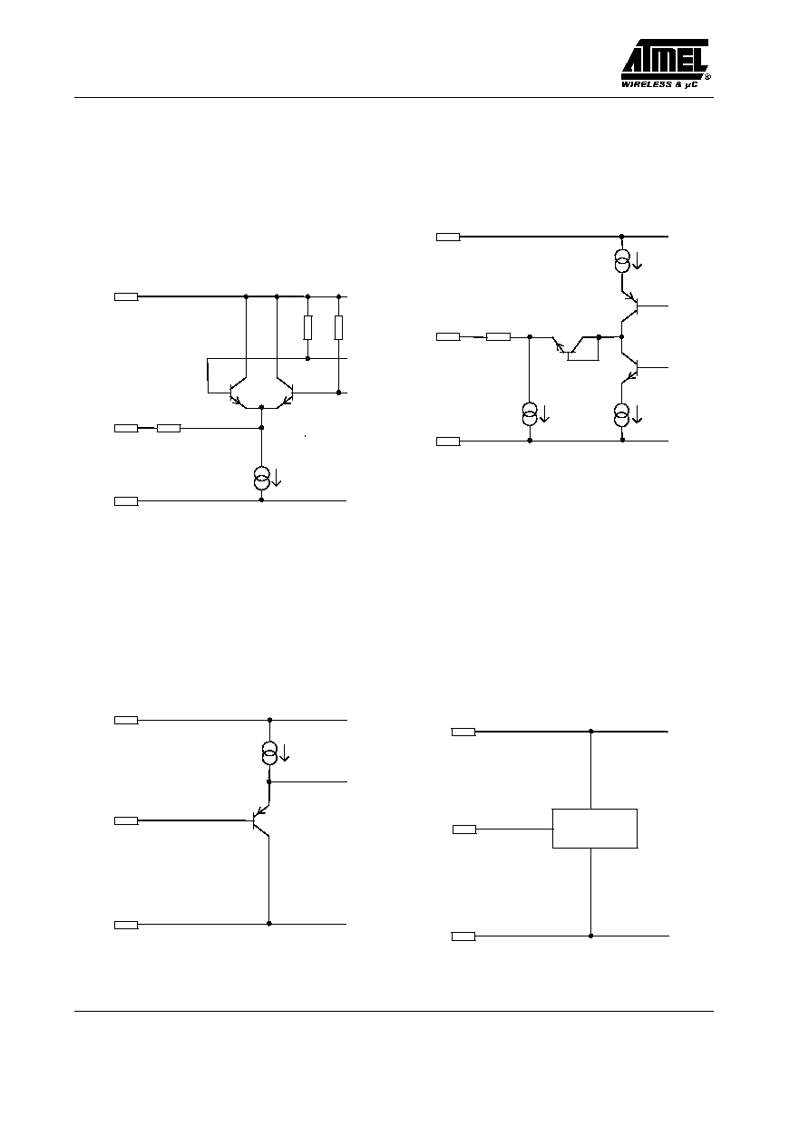
IN1, IN2
A ferrite antenna is connected between IN1 and IN2. For
high sensitivity, the Q factor of the antenna circuit should
be as high as possible. Please note that a high Q factor
requires temperature compensation of the resonant
frequency in most cases. We recommend a Q factor
between 80 and 150. An optimal signal-to-noise ratio will
be achieved by a resonant resistance of 40 k
W to 80 kW.
RF�Amp
200k
200k
from
AGC
GND
IN2
IN1
VCC
PAD 5
(Pin 6)
PAD 2
(Pin 3)
PAD 4
(Pin 5)
PAD 6
(Pin 7)
Figure 4.
RFO
In order to achieve a high selectivity, a crystal is
connected between the Pins RFO
and RFI. It is used with
the serial resonant frequency of to the time-code
transmitter (e.g., 60 kHz WWVB, 77.5 kHz DCF or
40 kHz JJY) and acts as a serial resonator. The equivalent
parallel capacitor of the filter crystal is internally
compensated so that the bandwidth of the filter is about
10 Hz. The impedance of RFI is high. Parasitic loads have
to be prevented.
55k
GND
RFO
VCC
PAD 2
(Pin 3)
PAD 4
(Pin 5)
PAD 3
(Pin 4)
Figure 5.
RFI
250k
GND
RFI
VCC
PAD 2
(Pin 3)
PAD 4
(Pin 5)
PAD 1
(Pin 2)
150k
Figure 6.
T4227
Rev. A3, 20-Mar-01
Preliminary Information
4 (14)
DEM
Demodulator output
To ensure the function, a external capacitor has to be
connected at this output. The value of the capacitor has be
adapted to the frequency of the received signal.
Frequencies below 70 kHz require a value of 68 nF to
100 nF, where as frequencies 70 kHz and above can work
with 47 nF to 68 nF.
GND
DEM
VCC
PAD 2
(Pin 3)
PAD 4
(Pin 5)
PAD12
(Pin15)
25k
Figure 7.
HLD
AGC hold mode: HLD high (V
SL
= V
CC
) sets normal
function, SL low (V
SL
= 0) holds for a short time the AGC
voltage. This can be used to prevent the AGC from peak
voltages, created by e.g., a stepper motor.
GND
HLD
VCC
PAD 2
(Pin 3)
PAD 4
(Pin 5)
PAD 11
(Pin 14)
Figure 8.
PK
Peak detector output: An external capacitor has to be
connected to ensure the function of the peak detector. The
value of the capacitance influences the AGC regulation
time.
GND
PK
VCC
PAD 2
(Pin 3)
PAD 4
(Pin 5)
PAD 10
(Pin 13)
from
Demodulator
Figure 9.
VCC, GND
VCC and GND are the supply voltage input. To power
down the circuitry it is recommended to use the PDN
input and not to switch the power supply. Switching the
power supply effects in a long power up waiting time.
PON
If PON is connected to GND, the receiver will be
activated. The set-up time is typically 0.5 s after applying
GND at this pin. If PON is connected to V
CC
, the receiver
will switch to power-down mode.
GND
PON
VCC
PAD 2
(Pin 3)
PAD 4
(Pin 5)
PAD 9
(Pin 12)
BIAS
Generator
Figure 10.
T4227
Preliminary Information
Rev. A3, 20-Mar-01
5 (14)
OUT1, OUT2
The serial signal of the time-code transmitter can be
directly decoded by a microcomputer. Details about the
time-code format of several transmitters are described
separately.
The output consists of a combination of a NPN / PNP open
collector stage. The function depends on the external
circuitry:
D A load resistor is connected from OUT1 to V
CC
,
OUT2 is connected to GND. This performs the func-
tionality of a NPN open collector stage.In this case,
the signal is active low.
D A load resistor is connected from OUT2 to GND,
OUT1 is connected to V
CC
. This performs the
functionality of a PNP open collector stage. In this
case, the signal is active high.
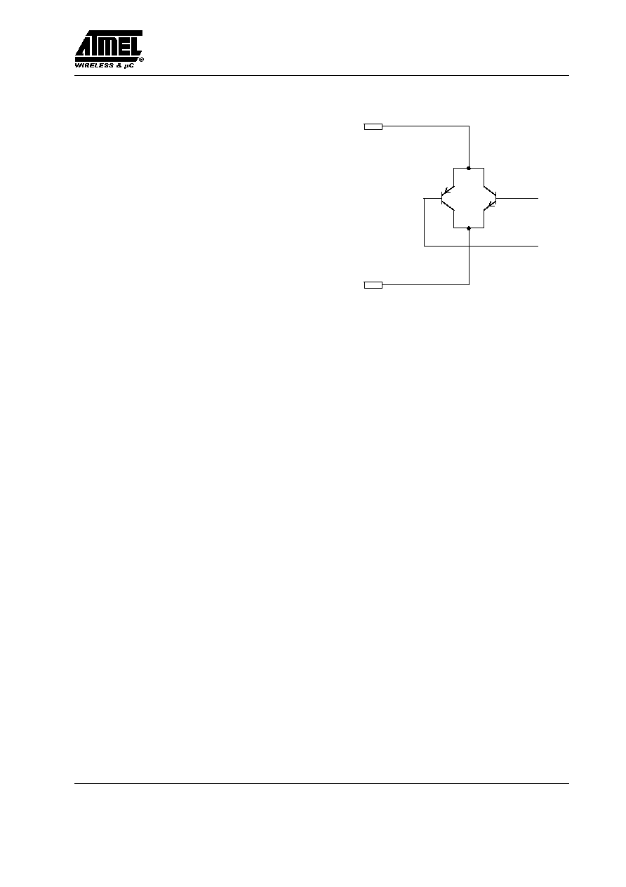
OUT2
OUT1
PAD 7
(Pin10)
PAD 8
(Pin11)
from
Comparator
Figure 11.