Document Outline
- Features / Benefits
- Table of Contents
- Ordering Information
- Introduction
- Differences between T48C894 and M44Cx90/x92
- Program Memory
- Configuration Memory
- Data Memory
- Reset Function
- MARC4 Architecture
- General Description
- Components of MARC4 Core
- Master Reset
- Voltage Monitor
- Clock Generation
- Power-down Modes
- Peripheral Modules
- Addressing Peripherals
- Bidirectional Ports
- Universal Timer/Counter / Communication Module (UTCM)
- Data EEPROM
- Electrical Characteristics
- Absolute Maximum Ratings
- DC Operating Characteristics
- AC Characteristics
- Package Information
- Selectable Options
T48C894
T48C894
Rev. A3, 22-Jan-02
1 (82)
8K-Flash Microcontroller
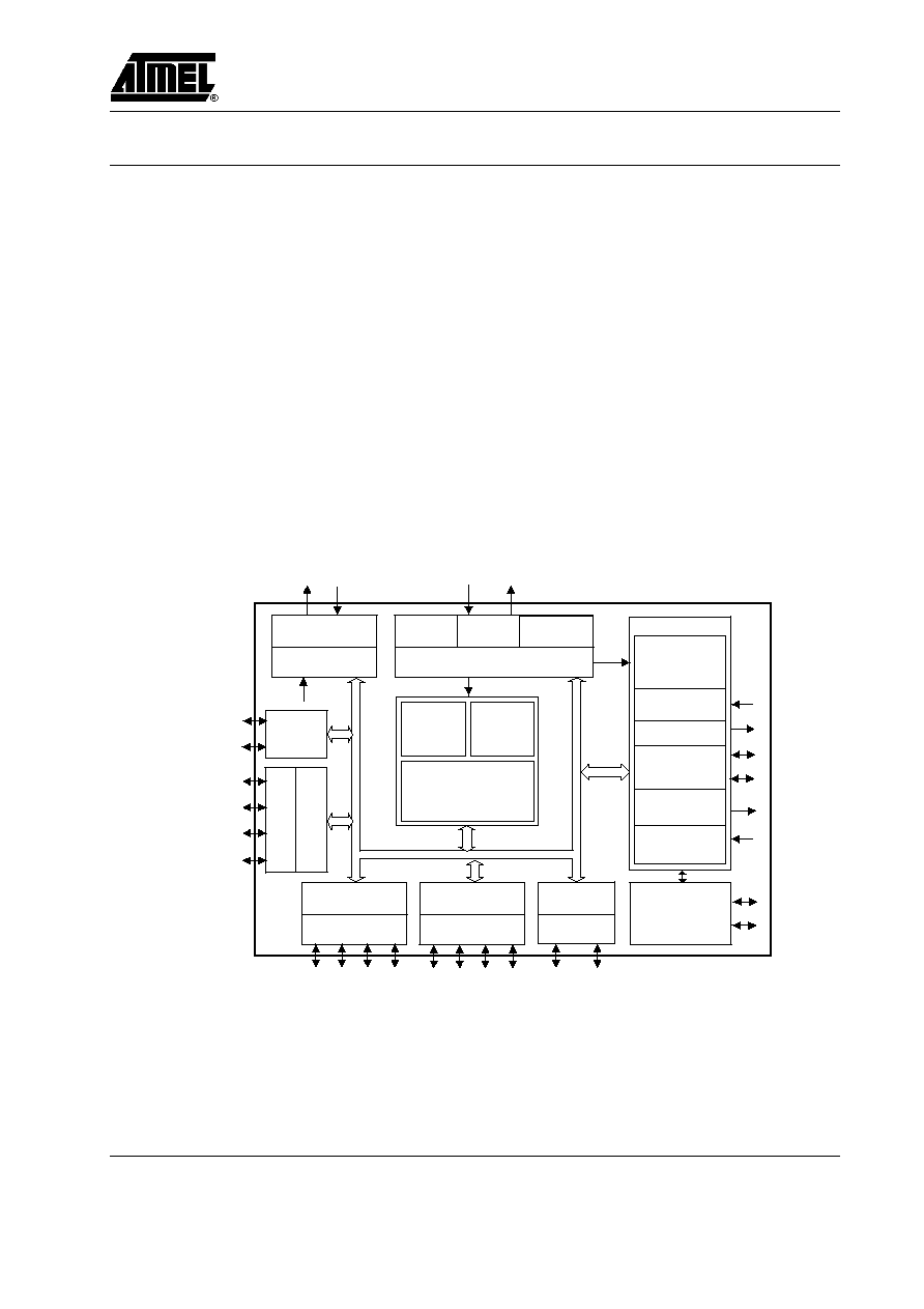
The T48C894 is a member of the Atmels family of 4-bit single chip microcontrollers with 8 K
8 bit EEPROM pro-
gram memory. It is based on the 4-K MTP version T48C893 and fully compatible with this MTP and the ROM versions
M44C090/890 and M44C092/892.
Features / Benefits
D 8 K 8 bit EEPROM
D EEPROM programmable options
D Read protection for the EEPROM program memory
D 256 4 bit RAM
D 2 32 16 bit data EEPROM
D Up to 7 external / internal interrupt sources
D 8 hardware and software interrupt priorities
D 16 bidirectional I/Os
D Wide supply-voltage range (1.8 to 6.5 V)
D Very low sleep current (< 1 µA)
D Synchronous serial interface (2-wire, I
2
C, 3-wire)
D Multifunction timer/counter with prescaler/interval
timer
D Voltage monitoring incl. Lo_BAT detect
D Watchdog, POR and brown-out function
Voltage monitor
External input
MARC4
UTCM
OSC1
OSC2
I/O bus
EEPROM
RAM
4-bit CPU core
256 x 4 bit
VDD
VSS
Data direction +
alternate function
Data direction +
interrupt control
Port 4
Port 5
Data dir. +
alt. function
Port 6
Timer 3
Brown-out protect.
RESET
Clock management
Timer 1
watchdog timer
Timer 2
Serial interface
Port 1
Port 2
Data direction
T2O
SD
SC
T3O
T3I
BP10
BP13
BP20/NTE
BP21
BP22
BP23
BP40
INT3
SC BP41
VMI
T2I
BP42
T2O BP43
INT3
SD
BP50
INT6
BP51
INT6
BP52
INT1
BP53
INT1
BP60
T3O
BP63
T3I
RC
oscillators
Crystal
oscillators
8 K x 8 bit
VMI
with prescaler
SSI
External
clock input
interval- and
timer / counter
T2I
EEPROM
2
32 16 bit
Modulator 2
Modulator 3
Demodulator
SD
SC
Figure 1. Block diagram T48C894
T48C894
Rev. A3, 22-Jan-02
2 (82)
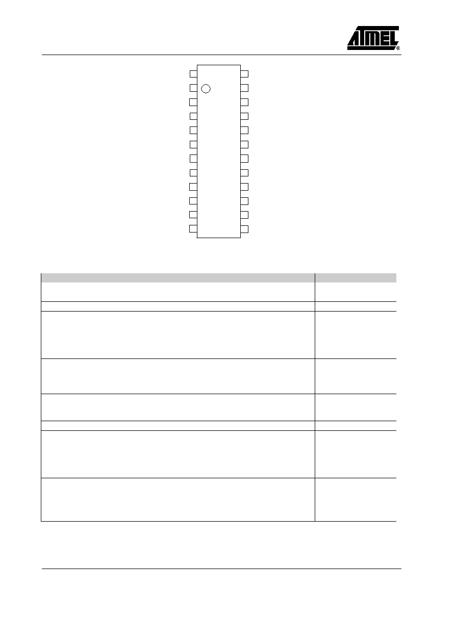
1
2
3
4
5
6
7
8
10
9
23
18
17
16
14
15
13
12
11
24
21
22
19
20
BP52/INT1
BP51/INT6
BP50/INT6
OSC1
OSC2
BP60/T3O
BP40/INT3/SC
BP53/INT1
BP10
VDD
n.c.
n.c.
BP41/VMI/T2I
BP23
BP22
BP21
BP20/NTE
BP63/T3I
BP43/INT3/SD
BP42/T2O
BP13
VSS
n.c.
n.c.
T48C894
Figure 2. Pinning SSO24 package
Table 1 Pin description
Name
Type
Function
Alternate Function
Pin-No.
Reset State
¡¡¡¡
V
DD
¡¡¡
¡¡¡¡¡¡¡¡¡¡
Supply voltage
¡¡¡¡¡¡¡¡¡¡
≠≠≠
¡¡¡¡
3
¡¡¡¡¡
NA
¡¡¡¡
¡¡¡¡
V
SS
¡¡¡
¡¡¡
¡¡¡¡¡¡¡¡¡¡
¡¡¡¡¡¡¡¡¡¡
Circuit ground
¡¡¡¡¡¡¡¡¡¡
¡¡¡¡¡¡¡¡¡¡
≠≠≠
¡¡¡¡
¡¡¡¡
22
¡¡¡¡¡
¡¡¡¡¡
NA
¡¡¡¡
¡¡¡¡
BP10
¡¡¡
¡¡¡
I/O
¡¡¡¡¡¡¡¡¡¡
¡¡¡¡¡¡¡¡¡¡
Bidirectional I/O line of Port 1.0
¡¡¡¡¡¡¡¡¡¡
¡¡¡¡¡¡¡¡¡¡
≠≠≠
¡¡¡¡
¡¡¡¡
12
¡¡¡¡¡
¡¡¡¡¡
Input
¡¡¡¡
¡¡¡¡
BP13
¡¡¡
¡¡¡
I/O
¡¡¡¡¡¡¡¡¡¡
¡¡¡¡¡¡¡¡¡¡
Bidirectional I/O line of Port 1.3
¡¡¡¡¡¡¡¡¡¡
¡¡¡¡¡¡¡¡¡¡
≠≠≠
¡¡¡¡
¡¡¡¡
13
¡¡¡¡¡
¡¡¡¡¡
Input
¡¡¡¡
¡¡¡¡
BP20
¡¡¡
¡¡¡
I/O
¡¡¡¡¡¡¡¡¡¡
¡¡¡¡¡¡¡¡¡¡
Bidirectional I/O line of Port 2.0
¡¡¡¡¡¡¡¡¡¡
¡¡¡¡¡¡¡¡¡¡
NTE≠test mode enable
¡¡¡¡
¡¡¡¡
15
¡¡¡¡¡
¡¡¡¡¡
Input
¡¡¡¡
BP21
¡¡¡
I/O
¡¡¡¡¡¡¡¡¡¡
Bidirectional I/O line of Port 2.1
¡¡¡¡¡¡¡¡¡¡
≠≠≠
¡¡¡¡
16
¡¡¡¡¡
Input
¡¡¡¡
¡¡¡¡
BP22
¡¡¡
¡¡¡
I/O
¡¡¡¡¡¡¡¡¡¡
¡¡¡¡¡¡¡¡¡¡
Bidirectional I/O line of Port 2.2
¡¡¡¡¡¡¡¡¡¡
¡¡¡¡¡¡¡¡¡¡
≠≠≠
¡¡¡¡
¡¡¡¡
17
¡¡¡¡¡
¡¡¡¡¡
Input
¡¡¡¡
¡¡¡¡
BP23
¡¡¡
¡¡¡
I/O
¡¡¡¡¡¡¡¡¡¡
¡¡¡¡¡¡¡¡¡¡
Bidirectional I/O line of Port 2.3
¡¡¡¡¡¡¡¡¡¡
¡¡¡¡¡¡¡¡¡¡
≠≠≠
¡¡¡¡
¡¡¡¡
18
¡¡¡¡¡
¡¡¡¡¡
Input
¡¡¡¡
¡¡¡¡
BP40
¡¡¡
¡¡¡
I/O
¡¡¡¡¡¡¡¡¡¡
¡¡¡¡¡¡¡¡¡¡
Bidirectional I/O line of Port 4.0
¡¡¡¡¡¡¡¡¡¡
¡¡¡¡¡¡¡¡¡¡
SC-serial clock or INT3 external inter-
rupt input
¡¡¡¡
¡¡¡¡
4
¡¡¡¡¡
¡¡¡¡¡
Input
¡¡¡¡
¡¡¡¡
¡¡¡¡
BP41
¡¡¡
¡¡¡
¡¡¡
I/O
¡¡¡¡¡¡¡¡¡¡
¡¡¡¡¡¡¡¡¡¡
¡¡¡¡¡¡¡¡¡¡
Bidirectional I/O line of Port 4.1
¡¡¡¡¡¡¡¡¡¡
¡¡¡¡¡¡¡¡¡¡
¡¡¡¡¡¡¡¡¡¡
VMI voltage monitor input or T2I ex-
ternal clock input Timer 2
¡¡¡¡
¡¡¡¡
¡¡¡¡
19
¡¡¡¡¡
¡¡¡¡¡
¡¡¡¡¡
Input
¡¡¡¡
¡¡¡¡
BP42
¡¡¡
¡¡¡
I/O
¡¡¡¡¡¡¡¡¡¡
¡¡¡¡¡¡¡¡¡¡
Bidirectional I/O line of Port 4.2
¡¡¡¡¡¡¡¡¡¡
¡¡¡¡¡¡¡¡¡¡
T2O Timer 2 output
¡¡¡¡
¡¡¡¡
20
¡¡¡¡¡
¡¡¡¡¡
Input
¡¡¡¡
¡¡¡¡
BP43
¡¡¡
¡¡¡
I/O
¡¡¡¡¡¡¡¡¡¡
¡¡¡¡¡¡¡¡¡¡
Bidirectional I/O line of Port 4.3
¡¡¡¡¡¡¡¡¡¡
¡¡¡¡¡¡¡¡¡¡
SD serial data I/O or INT3 external in-
terrupt input
¡¡¡¡
¡¡¡¡
21
¡¡¡¡¡
¡¡¡¡¡
Input
¡¡¡¡
¡¡¡¡
BP50
¡¡¡
¡¡¡
I/O
¡¡¡¡¡¡¡¡¡¡
¡¡¡¡¡¡¡¡¡¡
Bidirectional I/O line of Port 5.0
¡¡¡¡¡¡¡¡¡¡
¡¡¡¡¡¡¡¡¡¡
INT6 external interrupt input
¡¡¡¡
¡¡¡¡
8
¡¡¡¡¡
¡¡¡¡¡
Input
¡¡¡¡
¡¡¡¡
BP51
¡¡¡
¡¡¡
I/O
¡¡¡¡¡¡¡¡¡¡
¡¡¡¡¡¡¡¡¡¡
Bidirectional I/O line of Port 5.1
¡¡¡¡¡¡¡¡¡¡
¡¡¡¡¡¡¡¡¡¡
INT6 external interrupt input
¡¡¡¡
¡¡¡¡
7
¡¡¡¡¡
¡¡¡¡¡
Input
¡¡¡¡
¡¡¡¡
BP52
¡¡¡
¡¡¡
I/O
¡¡¡¡¡¡¡¡¡¡
¡¡¡¡¡¡¡¡¡¡
Bidirectional I/O line of Port 5.2
¡¡¡¡¡¡¡¡¡¡
¡¡¡¡¡¡¡¡¡¡
INT1 external interrupt input
¡¡¡¡
¡¡¡¡
6
¡¡¡¡¡
¡¡¡¡¡
Input
¡¡¡¡
¡¡¡¡
BP53
¡¡¡
¡¡¡
I/O
¡¡¡¡¡¡¡¡¡¡
¡¡¡¡¡¡¡¡¡¡
Bidirectional I/O line of Port 5.3
¡¡¡¡¡¡¡¡¡¡
¡¡¡¡¡¡¡¡¡¡
INT1 external interrupt input
¡¡¡¡
¡¡¡¡
5
¡¡¡¡¡
¡¡¡¡¡
Input
¡¡¡¡
BP60
¡¡¡
I/O
¡¡¡¡¡¡¡¡¡¡
Bidirectional I/O line of Port 6.0
¡¡¡¡¡¡¡¡¡¡
T3O Timer 3 output
¡¡¡¡
11
¡¡¡¡¡
Input
¡¡¡¡
¡¡¡¡
BP63
¡¡¡
¡¡¡
I/O
¡¡¡¡¡¡¡¡¡¡
¡¡¡¡¡¡¡¡¡¡
Bidirectional I/O line of Port 6.3
¡¡¡¡¡¡¡¡¡¡
¡¡¡¡¡¡¡¡¡¡
T3I Timer 3 input
¡¡¡¡
¡¡¡¡
14
¡¡¡¡¡
¡¡¡¡¡
Input
¡¡¡¡
¡¡¡¡
¡¡¡¡
OSC1
¡¡¡
¡¡¡
¡¡¡
I
¡¡¡¡¡¡¡¡¡¡
¡¡¡¡¡¡¡¡¡¡
¡¡¡¡¡¡¡¡¡¡
Oscillator input
¡¡¡¡¡¡¡¡¡¡
¡¡¡¡¡¡¡¡¡¡
¡¡¡¡¡¡¡¡¡¡
4-MHz crystal input or 32-kHz crystal
input or external clock input or exter-
nal trimming resistor input
¡¡¡¡
¡¡¡¡
¡¡¡¡
9
¡¡¡¡¡
¡¡¡¡¡
¡¡¡¡¡
Input
¡¡¡¡
¡¡¡¡
¡¡¡¡
OSC2
¡¡¡
¡¡¡
¡¡¡
O
¡¡¡¡¡¡¡¡¡¡
¡¡¡¡¡¡¡¡¡¡
¡¡¡¡¡¡¡¡¡¡
Oscillator output
¡¡¡¡¡¡¡¡¡¡
¡¡¡¡¡¡¡¡¡¡
¡¡¡¡¡¡¡¡¡¡
4-MHz crystal output or 32-kHz crys-
tal output or external clock input
¡¡¡¡
¡¡¡¡
¡¡¡¡
10
¡¡¡¡¡
¡¡¡¡¡
¡¡¡¡¡
Input

T48C894
T48C894
Rev. A3, 22-Jan-02
3 (82)
Table of Contents
1
Introduction
6
. . . . . . . . . . . . . . . . . . . . . . . . . . . . . . . . . . . . . . . . . . . . . . . . . . . . . . . . . . . . . . . . . . . . . .
2
Differences between T48C894 and M44Cx90/x92
6
. . . . . . . . . . . . . . . . . . . . . . . . . . . . . . . . . . . . . . .
2.1
Program Memory
6
. . . . . . . . . . . . . . . . . . . . . . . . . . . . . . . . . . . . . . . . . . . . . . . . . . . . . . . . . . .
2.2
Configuration Memory
6
. . . . . . . . . . . . . . . . . . . . . . . . . . . . . . . . . . . . . . . . . . . . . . . . . . . . . . .
2.3
Data Memory
6
. . . . . . . . . . . . . . . . . . . . . . . . . . . . . . . . . . . . . . . . . . . . . . . . . . . . . . . . . . . . . .
2.4
Reset Function
6
. . . . . . . . . . . . . . . . . . . . . . . . . . . . . . . . . . . . . . . . . . . . . . . . . . . . . . . . . . . . .
3
MARC4 Architecture
7
. . . . . . . . . . . . . . . . . . . . . . . . . . . . . . . . . . . . . . . . . . . . . . . . . . . . . . . . . . . . . .
3.1
General Description
7
. . . . . . . . . . . . . . . . . . . . . . . . . . . . . . . . . . . . . . . . . . . . . . . . . . . . . . . . .
3.2
Components of MARC4 Core
8
. . . . . . . . . . . . . . . . . . . . . . . . . . . . . . . . . . . . . . . . . . . . . . . . .
3.2.1
Program Memory
8
. . . . . . . . . . . . . . . . . . . . . . . . . . . . . . . . . . . . . . . . . . . . . . . . . .
3.2.2
RAM
8
. . . . . . . . . . . . . . . . . . . . . . . . . . . . . . . . . . . . . . . . . . . . . . . . . . . . . . . . . . . .
3.2.3
Registers
9
. . . . . . . . . . . . . . . . . . . . . . . . . . . . . . . . . . . . . . . . . . . . . . . . . . . . . . . . .
3.2.4
ALU
11
. . . . . . . . . . . . . . . . . . . . . . . . . . . . . . . . . . . . . . . . . . . . . . . . . . . . . . . . . . . . .
3.2.5
I/O Bus
11
. . . . . . . . . . . . . . . . . . . . . . . . . . . . . . . . . . . . . . . . . . . . . . . . . . . . . . . . . .
3.2.6
Instruction Set
11
. . . . . . . . . . . . . . . . . . . . . . . . . . . . . . . . . . . . . . . . . . . . . . . . . . . . .
3.2.7
Interrupt Structure
11
. . . . . . . . . . . . . . . . . . . . . . . . . . . . . . . . . . . . . . . . . . . . . . . . . .
Software Interrupts
13
. . . . . . . . . . . . . . . . . . . . . . . . . . . . . . . . . . . . . . . . . . . . . . . . .
Hardware Interrupts
13
. . . . . . . . . . . . . . . . . . . . . . . . . . . . . . . . . . . . . . . . . . . . . . . .
3.3
Master Reset
13
. . . . . . . . . . . . . . . . . . . . . . . . . . . . . . . . . . . . . . . . . . . . . . . . . . . . . . . . . . . . . . .
3.3.1
Power-on Reset and Brown-out Detection
14
. . . . . . . . . . . . . . . . . . . . . . . . . . . . . . .
3.3.2
Watchdog Reset
15
. . . . . . . . . . . . . . . . . . . . . . . . . . . . . . . . . . . . . . . . . . . . . . . . . . .
3.3.3
External Clock Supervisor
15
. . . . . . . . . . . . . . . . . . . . . . . . . . . . . . . . . . . . . . . . . . .
3.4
Voltage Monitor
15
. . . . . . . . . . . . . . . . . . . . . . . . . . . . . . . . . . . . . . . . . . . . . . . . . . . . . . . . . . . .
3.4.1
Voltage Monitor Control / Status Register
16
. . . . . . . . . . . . . . . . . . . . . . . . . . . . . . .
3.5
Clock Generation
17
. . . . . . . . . . . . . . . . . . . . . . . . . . . . . . . . . . . . . . . . . . . . . . . . . . . . . . . . . . .
3.5.1
Clock Module
17
. . . . . . . . . . . . . . . . . . . . . . . . . . . . . . . . . . . . . . . . . . . . . . . . . . . . .
3.5.2
Oscillator Circuits and External Clock Input Stage
18
. . . . . . . . . . . . . . . . . . . . . . . .
RC-Oscillator 1 Fully Integrated
18
. . . . . . . . . . . . . . . . . . . . . . . . . . . . . . . . . . . . . .
External Input Clock
18
. . . . . . . . . . . . . . . . . . . . . . . . . . . . . . . . . . . . . . . . . . . . . . . .
RC-Oscillator 2 with External Trimming Resistor
18
. . . . . . . . . . . . . . . . . . . . . . . . .
4-MHz Oscillator
18
. . . . . . . . . . . . . . . . . . . . . . . . . . . . . . . . . . . . . . . . . . . . . . . . . .
32-kHz Oscillator
19
. . . . . . . . . . . . . . . . . . . . . . . . . . . . . . . . . . . . . . . . . . . . . . . . . .
3.5.3
Clock Management
19
. . . . . . . . . . . . . . . . . . . . . . . . . . . . . . . . . . . . . . . . . . . . . . . . .
Clock Management Register (CM)
19
. . . . . . . . . . . . . . . . . . . . . . . . . . . . . . . . . . . . .
System Configuration Register (SC)
20
. . . . . . . . . . . . . . . . . . . . . . . . . . . . . . . . . . .
3.6
Power-down Modes
20
. . . . . . . . . . . . . . . . . . . . . . . . . . . . . . . . . . . . . . . . . . . . . . . . . . . . . . . . . .
4
Peripheral Modules
21
. . . . . . . . . . . . . . . . . . . . . . . . . . . . . . . . . . . . . . . . . . . . . . . . . . . . . . . . . . . . . . .
4.1
Addressing Peripherals
21
. . . . . . . . . . . . . . . . . . . . . . . . . . . . . . . . . . . . . . . . . . . . . . . . . . . . . . .
4.2
Bidirectional Ports
23
. . . . . . . . . . . . . . . . . . . . . . . . . . . . . . . . . . . . . . . . . . . . . . . . . . . . . . . . . .
4.2.1
Bidirectional Port 1
23
. . . . . . . . . . . . . . . . . . . . . . . . . . . . . . . . . . . . . . . . . . . . . . . . .
4.2.2
Bidirectional Port 2
24
. . . . . . . . . . . . . . . . . . . . . . . . . . . . . . . . . . . . . . . . . . . . . . . . .
Port 2 Data Register (P2DAT)
24
. . . . . . . . . . . . . . . . . . . . . . . . . . . . . . . . . . . . . . . .
Port 2 Control Register (P2CR)
24
. . . . . . . . . . . . . . . . . . . . . . . . . . . . . . . . . . . . . . .

T48C894
Rev. A3, 22-Jan-02
4 (82)
Table of Contents (continued)
4.2.3
Bidirectional Port 5
25
. . . . . . . . . . . . . . . . . . . . . . . . . . . . . . . . . . . . . . . . . . . . . . . . .
4.2.4
Bidirectional Port 4
27
. . . . . . . . . . . . . . . . . . . . . . . . . . . . . . . . . . . . . . . . . . . . . . . . .
4.2.5
Bidirectional Port 6
28
. . . . . . . . . . . . . . . . . . . . . . . . . . . . . . . . . . . . . . . . . . . . . . . . .
4.3
Universal Timer/Counter / Communication Module (UTCM)
29
. . . . . . . . . . . . . . . . . . . . . . . .
4.3.1
Timer 1
30
. . . . . . . . . . . . . . . . . . . . . . . . . . . . . . . . . . . . . . . . . . . . . . . . . . . . . . . . . .
Timer 1 Control Register 1 (T1C1)
31
. . . . . . . . . . . . . . . . . . . . . . . . . . . . . . . . . . . .
Timer 1 Control Register 2 (T1C2)
31
. . . . . . . . . . . . . . . . . . . . . . . . . . . . . . . . . . . .
Watchdog Control Register (WDC)
32
. . . . . . . . . . . . . . . . . . . . . . . . . . . . . . . . . . . .
4.3.2
Timer 2
32
. . . . . . . . . . . . . . . . . . . . . . . . . . . . . . . . . . . . . . . . . . . . . . . . . . . . . . . . . .
Timer 2 Modes
33
. . . . . . . . . . . . . . . . . . . . . . . . . . . . . . . . . . . . . . . . . . . . . . . . . . . .
Timer 2 Output Modes
34
. . . . . . . . . . . . . . . . . . . . . . . . . . . . . . . . . . . . . . . . . . . . . .
Timer 2 Output Signals
35
. . . . . . . . . . . . . . . . . . . . . . . . . . . . . . . . . . . . . . . . . . . . . .
Timer 2 Registers
38
. . . . . . . . . . . . . . . . . . . . . . . . . . . . . . . . . . . . . . . . . . . . . . . . . .
Timer 2 Control Register (T2C)
38
. . . . . . . . . . . . . . . . . . . . . . . . . . . . . . . . . . . . . . .
Timer 2 Mode Register 1 (T2M1)
39
. . . . . . . . . . . . . . . . . . . . . . . . . . . . . . . . . . . . .
Timer 2 Mode Register 2 (T2M2)
40
. . . . . . . . . . . . . . . . . . . . . . . . . . . . . . . . . . . . .
Timer 2 Compare and Compare Mode Registers
41
. . . . . . . . . . . . . . . . . . . . . . . . . .
Timer 2 Compare Mode Register (T2CM)
41
. . . . . . . . . . . . . . . . . . . . . . . . . . . . . . .
Timer 2 COmpare Register 1 (T2CO1)
41
. . . . . . . . . . . . . . . . . . . . . . . . . . . . . . . . .
Timer 2 COmpare Register 2 (T2CO2) Byte Write
41
. . . . . . . . . . . . . . . . . . . . . . . .
4.3.3
Timer 3
42
. . . . . . . . . . . . . . . . . . . . . . . . . . . . . . . . . . . . . . . . . . . . . . . . . . . . . . . . . .
Timer / Counter Modes
43
. . . . . . . . . . . . . . . . . . . . . . . . . . . . . . . . . . . . . . . . . . . . . .
Timer 3 Modulator / Demodulator Modes
45
. . . . . . . . . . . . . . . . . . . . . . . . . . . . . . .
Timer 3 Modulator for Carrier Frequency Burst Modulation
48
. . . . . . . . . . . . . . . .
Timer 3 Demodulator for Biphase, Manchester and Pulse-Width-Modulated Signals
48
Timer 3 Registers
49
. . . . . . . . . . . . . . . . . . . . . . . . . . . . . . . . . . . . . . . . . . . . . . . . . .
Timer 3 Mode Register (T3M)
49
. . . . . . . . . . . . . . . . . . . . . . . . . . . . . . . . . . . . . . .
Timer 3 Control Register 1 (T3C) Write
49
. . . . . . . . . . . . . . . . . . . . . . . . . . . . . . . .
Timer 3 Status Register 1 (T3ST) Read
50
. . . . . . . . . . . . . . . . . . . . . . . . . . . . . . . . .
Timer 3 Clock Select Register (T3CS)
50
. . . . . . . . . . . . . . . . . . . . . . . . . . . . . . . . . .
Timer 3 Compare- and Compare Mode Register
50
. . . . . . . . . . . . . . . . . . . . . . . . . .
Timer 3 Compare Mode Register 1 (T3CM1)
51
. . . . . . . . . . . . . . . . . . . . . . . . . . . .
Timer 3 Compare Mode Register 2 (T3CM2)
51
. . . . . . . . . . . . . . . . . . . . . . . . . . . .
Timer 3 COmpare Register 1 (T3CO1) Byte Write
52
. . . . . . . . . . . . . . . . . . . . . . . .
Timer 3 COmpare Register 2 (T3CO2) Byte Write
52
. . . . . . . . . . . . . . . . . . . . . . . .
Timer 3 Capture register
52
. . . . . . . . . . . . . . . . . . . . . . . . . . . . . . . . . . . . . . . . . . . . .
Timer 3 CaPture Register (T3CP) Byte Read
52
. . . . . . . . . . . . . . . . . . . . . . . . . . . .
4.3.4
Synchronous Serial Interface (SSI)
53
. . . . . . . . . . . . . . . . . . . . . . . . . . . . . . . . . . . . .
SSI Peripheral Configuration
53
. . . . . . . . . . . . . . . . . . . . . . . . . . . . . . . . . . . . . . . . .
General SSI Operation
54
. . . . . . . . . . . . . . . . . . . . . . . . . . . . . . . . . . . . . . . . . . . . . .
8-bit Synchronous Mode
55
. . . . . . . . . . . . . . . . . . . . . . . . . . . . . . . . . . . . . . . . . . . . .
9-bit Shift Mode (I2C compatible)
56
. . . . . . . . . . . . . . . . . . . . . . . . . . . . . . . . . . . . .

T48C894
T48C894
Rev. A3, 22-Jan-02
5 (82)
Table of Contents (continued)
8-bit Pseudo I2C Mode
57
. . . . . . . . . . . . . . . . . . . . . . . . . . . . . . . . . . . . . . . . . . . . . .
I2C Bus Protocol
57
. . . . . . . . . . . . . . . . . . . . . . . . . . . . . . . . . . . . . . . . . . . . . . . . . . .
SSI Interrupt
59
. . . . . . . . . . . . . . . . . . . . . . . . . . . . . . . . . . . . . . . . . . . . . . . . . . . . . .
Modulation and Demodulation
59
. . . . . . . . . . . . . . . . . . . . . . . . . . . . . . . . . . . . . . . .
Internal 2-Wire Multi-Chip Link
59
. . . . . . . . . . . . . . . . . . . . . . . . . . . . . . . . . . . . . .
Serial Interface Registers
60
. . . . . . . . . . . . . . . . . . . . . . . . . . . . . . . . . . . . . . . . . . . .
Serial Interface Control Register 1 (SIC1)
60
. . . . . . . . . . . . . . . . . . . . . . . . . . . . . . .
Serial Interface Control Register 2 (SIC2)
60
. . . . . . . . . . . . . . . . . . . . . . . . . . . . . . .
Serial Interface Status and Control Register (SISC)
61
. . . . . . . . . . . . . . . . . . . . . . .
Serial Transmit Buffer (STB) ≠ Byte Write
61
. . . . . . . . . . . . . . . . . . . . . . . . . . . . . .
Serial Receive Buffer (SRB) ≠ Byte Read
62
. . . . . . . . . . . . . . . . . . . . . . . . . . . . . . .
4.3.5
Combination Modes
62
. . . . . . . . . . . . . . . . . . . . . . . . . . . . . . . . . . . . . . . . . . . . . . . .
Combination Mode Timer 2 and SSI
62
. . . . . . . . . . . . . . . . . . . . . . . . . . . . . . . . . . .
Combination Mode Timer 3 and SSI
65
. . . . . . . . . . . . . . . . . . . . . . . . . . . . . . . . . . .
Combination Mode Timer 2 and Timer 3
68
. . . . . . . . . . . . . . . . . . . . . . . . . . . . . . . .
Combination Mode Timer 2, Timer 3 and SSI
70
. . . . . . . . . . . . . . . . . . . . . . . . . . . .
5
Data EEPROM
72
. . . . . . . . . . . . . . . . . . . . . . . . . . . . . . . . . . . . . . . . . . . . . . . . . . . . . . . . . . . . . . . . . . .
5.1
Serial Interface
73
. . . . . . . . . . . . . . . . . . . . . . . . . . . . . . . . . . . . . . . . . . . . . . . . . . . .
Serial Protocol
73
. . . . . . . . . . . . . . . . . . . . . . . . . . . . . . . . . . . . . . . . . . . . . . . . . . . . .
5.1.1
EEPROM
74
. . . . . . . . . . . . . . . . . . . . . . . . . . . . . . . . . . . . . . . . . . . . . . . . . . . . . . . . .
EEPROM ≠ Operating Modes
74
. . . . . . . . . . . . . . . . . . . . . . . . . . . . . . . . . . . . . . . .
Write Operations
74
. . . . . . . . . . . . . . . . . . . . . . . . . . . . . . . . . . . . . . . . . . . . . . . . . . .
Read Operations
75
. . . . . . . . . . . . . . . . . . . . . . . . . . . . . . . . . . . . . . . . . . . . . . . . . . .
Initialization the Serial Interface to the EEPROM
75
. . . . . . . . . . . . . . . . . . . . . . . . .
6
Electrical Characteristics
76
. . . . . . . . . . . . . . . . . . . . . . . . . . . . . . . . . . . . . . . . . . . . . . . . . . . . . . . . . .
6.1
Absolute Maximum Ratings
76
. . . . . . . . . . . . . . . . . . . . . . . . . . . . . . . . . . . . . . . . . . . . . . . . . . .
6.2
DC Operating Characteristics
76
. . . . . . . . . . . . . . . . . . . . . . . . . . . . . . . . . . . . . . . . . . . . . . . . . .
6.3
AC Characteristics
78
. . . . . . . . . . . . . . . . . . . . . . . . . . . . . . . . . . . . . . . . . . . . . . . . . . . . . . . . . .
7
Package Information
80
. . . . . . . . . . . . . . . . . . . . . . . . . . . . . . . . . . . . . . . . . . . . . . . . . . . . . . . . . . . . . .
8
Selectable Options
81
. . . . . . . . . . . . . . . . . . . . . . . . . . . . . . . . . . . . . . . . . . . . . . . . . . . . . . . . . . . . . . . .