 | –≠–ª–µ–∫—Ç—Ä–æ–Ω–Ω—ã–π –∫–æ–º–ø–æ–Ω–µ–Ω—Ç: T5760 | –°–∫–∞—á–∞—Ç—å:  PDF PDF  ZIP ZIP |

T5761
T5760 /
Preliminary Information
Rev. A2, 19-Oct-00
1 (32)
UHF ASK/FSK Receiver
Description
The T5760/T5761 is a multi-chip PLL receiver device
supplied in an SO20 package. It has been especially de-
veloped for the demands of RF low-cost data transmission
systems with data rates from 1 kBaud to 10 kBaud in
Manchester or Bi-phase code. The receiver is well suited
to operate with the Atmel Wireless & Microcontrollers'
PLL RF transmitter T5750. Its main applications are in
the areas of telemetering, security technology and key-
less-entry systems. It can be used in the frequency
receiving range of f
0
= 868 to 870 MHz or f
0
= 902 to
928 MHz for ASK or FSK data transmission. All the
statements made below refer to 868.3 MHz and
915.0 MHz applications.
Features
D Fully integrated LC-VCO and PLL loop filter
D Very high sensitivity with power matched LNA
D 30 dB image rejection
D High system IIP3 (≠16 dBm), system 1-dB compres-
sion point (≠25 dBm)
D High large-signal capability at GSM band (blocking
≠30 dBm @ + 20 MHz, IIP3 = ≠12 dBm @ + 20 MHz)
D 5 V to 20 V automotive compatible data interface
D Data clock available for Manchester- and Bi-phase-
coded signals
D Programmable digital noise suppresion
D Receiving bandwidth B
IF
= 600 kHz for low cost
90-ppm crystals
D Low power consumption due to configurable polling
D Temperature range ≠40
∞
C to 105
∞
C
D ESD protection 2 kV HBM, 200 V MM
D Communication to mC possible via a single
bi-directional data line
D Low-cost solution due to high integration level with
minimum external circuitry requirements
System Block Diagram
Demod.
IF Amp
LNA
VCO
PLL
XTO
Control
T5760/
T5761
1...5
mC
Power
amp.
XTO
VCO
PLL
T5750
Antenna
Antenna
UHF ASK/FSK
Remote control transmitter
UHF ASK/FSK
Remote control receiver
Figure 1. System block diagram
Ordering Information
Extended Type Number
Package
Remarks
T5760-TG
SO20
Tube, for 868 MHz ISM band
T5760-TGQ
SO20
Taped and reeled, for 868 MHz ISM band
T5761-TG
SO20
Tube, for 915 MHz ISM band
T5761-TGQ
SO20
Taped and reeled, for 915 MHz ISM band

T5760 T5761
/
Rev. A2, 19-Oct-00
Preliminary Information
2 (32)
Pin Description
Pin
Symbol
Function
1
SENS
Sensitivity-control resistor
2
IC_
ACTIVE
IC condition indicator
Low = sleep mode
High = active mode
3
CDEM
Lower cut-off frequency data fil-
ter
4
AVCC
Analog power supply
5
TEST 1
Test pin, during operation at GND
6
AGND
Analog ground
7
n.c.
Not connected, connect to GND
8
LNAREF
High-frequency reference node
LNA and mixer
9
LNA_IN
RF input
10
LNAGND DC ground LNA and mixer
11
TEST 2
Do not connect during operating
12
TEST 3
Test pin, during operation at GND
13
n.c.
Not connected, connect to GND
14
XTAL
Crystal oscillator XTAL connec-
tion
15
DVCC
Digital power supply
16
TEST 4
Test pin, during operation at
DVCC
17
DATA_
CLK
Bit clock of data stream
18
DGND
Digital ground
19
POLL-
ING/_ON
Selects polling or rceiving mode
Low: receiving mode
High: polling mode
20
DATA
Data output / configuration input
1
2
3
4
5
6
7
8
10
9
19
18
17
16
14
15
13
12
11
20
AVCC
TEST 1
AGND
n.c.
LNAREF
LNA_IN
IC_ACTIVE
CDEM
DATA_CLK
TEST 4
XTAL
n.c.
TEST 3
POLLING
/_ON
DGND
LNAGND
TEST 2
DATA
DVCC
SENS
T5760/
T5761
Figure 2. Pinning SO20

T5761
T5760 /
Preliminary Information
Rev. A2, 19-Oct-00
3 (32)
Block Diagram
SENS
CDEM
AVCC
AGND
DGND
LNAGND
LNA_IN
DATA
POLLING/_ON
DATA_CLK
DVCC
XTAL
Polling circuit
and
control logic
Rssi
Limiter out
LC≠VCO
f
:256
XTO
Standby logic
FE
CLK
FSK/ASK≠
demodulator
and data filter
RSSI IF
Amp.
Poly≠LPF
fg=7MHz
LNA
4. Order
f0=950 kHz/
Dem_out
Sensitivity≠
reduction
LPF
fg=2.2MHz
IF
Amp.
IC_ACTIVE
Data ≠
interface
LNAREF
f
:2
Loop≠
filter
1 MHz
Figure 3. Block diagram
RF Front End
The RF front end of the receiver is a low-IF heterodyne
configuration that converts the input signal into a
950-kHz/ 1-MHz IF signal with an image rejection of typ-
ical 30dB. According to figure 3 the front end consists of
an LNA (low noise amplifier), LO (local oscillator), I/Q
mixer, polyphase lowpass filter and an IF amplifier.
The PLL generates the carrier frequency for the mixer via
a full integrated synthesizer with integrated low noise
LC-VCO (voltage controlled oscillator ) and PLL-loop-
filter. The XTO ( crystal oscillator ) generates the
reference frequency f
XTO
. The integrated LC-VCO gen-
erates two times the mixer drive frequency f
VCO
. The I/Q
signals for the mixer are generated with a divide by two
circuit ( f
LO
= f
VCO
/2 ). f
VCO
is divided by a factor of 256
and feed into a phase frequency detector and compared
with f
XTO
. The output of the phase frequency detector is
feed into an integrated loopfilter and thereby generates
the control voltage for the VCO. If f
LO
is determined,
f
XTO
can be calculated using the following formula:
f
XTO
= f
LO
/ 128
The XTO is a one-pin oscillator that operates at the series
resonance of the quartz crystal with high current but low
voltage signal, so that there is only a small voltage at the
crystal oscillator frequency at Pin XTAL. According to
figure 4, the crystal should be connected to GND with a
series capacitor C
L
. The value of that capacitor is recom-
mended by the crystal supplier. Due to a somewhat
inductive impedance at steady state oscillation and some
PCB parasitics a lower value of C
L
is normally necessary.
T5760 T5761
/
Rev. A2, 19-Oct-00
Preliminary Information
4 (32)
The value of C
L
should be optimized for the individual
board layout to achieve the exact value of f
XTO
(the best
way is to use a crystal with known load resonance fre-
quency to find the right value for this capacitor) and
hereby of f
LO
. When designing the system in terms of re-
ceiving bandwidth and local oscillator accuracy, the
accuracy of the crystal and the XTO must be considered.
If a crystal with
$30 ppm adjustment tolerance at 25_C
,
$50ppm over Temperature ≠40_C to 105_C, $10 ppm
of total aging and a CM ( motional capacitance ) of 7 fF
is used, an additional XTO pulling of
$30 ppm has to be
added.
The resulting total LO tolerance of
$120ppm agrees with
the receiving bandwidth specification of the
T5760/T5761 if the T5750 has also a total LO tolerance
of
$120 ppm.
DVCC
XTAL
TEST 3
TEST 2
n.c.
V
C
S
L
Figure 4. XTO peripherals
The nominal frequency f
LO
is determined by the RF input
frequency f
RF
and the IF frequency f
IF
using the following
formula (low side injection):
f
LO
= f
RF
≠ f
IF
To determine f
LO
, the construction of the IF filter must
be considered at this point. The nominal IF frequency is
f
IF
= 950 kHz. To achieve a good accuracy of the filter
corner frequencies, the filter is tuned by the crystal fre-
quency f
XTO
. This means that there is a fixed relation
between f
IF
and f
LO
.
f
IF
= f
LO
/ 915
The relation is designed to achieve the nominal IF fre-
quency of f
IF
= 950 kHz for the 868.3 MHz version. For
the 915 MHz version an IF frequency of f
IF
= 1.0 MHz
results.
The RF input either from an antenna or from a RF genera-
tor must be transformed to the RF input Pin LNA_IN. The
input impedance of that pin is provided in the electrical
parameters. The parasitic board inductances and capaci-
tances influence the input matching. The RF receiver
T5760/T5761 exhibits its highest sensitivity if the LNA
is power matched. This makes the matching to an SAW
filter as well as to 50
W or an antenna more easy.
Figure 33 shows a typical input matching network for f
RF
= 868.3 MHz to 50
W. Figure 34 illustrates an according
input matching for 868.3 MHz to an SAW. The input
matching network shown in Figure 33 is the reference net-
work for the parameters given in the electrical
characteristics.
Analog Signal Processing
IF Filter
The signals coming from the RF front end are filtered by
the fully integrated 4th-order IF filter. The IF center fre-
quency is f
IF
= 950 kHz for applications where f
RF
=
868.3 MHz and f
IF
=1.0 MHz for f
RF
= 915 MHz. The
nominal bandwidth is 600 kHz.
Limiting RSSI Amplifier
The subsequent RSSI amplifier enhances the output
signal of the IF amplifier before it is fed into the demod-
ulator. The dynamic range of this amplifier is
DR
RSSI
= 60 dB. If the RSSI amplifier is operated within
its linear range, the best S/N ratio is maintained in ASK
mode. If the dynamic range is exceeded by the transmitter
signal, the S/N ratio is defined by the ratio of the maxi-
mum RSSI output voltage and the RSSI output voltage
due to a disturber. The dynamic range of the RSSI ampli-
fier is exceeded if the RF input signal is about 60 dB
higher compared to the RF input signal at full sensitivity.
In FSK mode the S/N ratio is not affected by the dynamic
range of the RSSI amplifier, because only the hard limited
signal from a high gain limiting amplifier is used by the
demodulator.
The output voltage of the RSSI amplifier is internally
compared to a threshold voltage V
Th_red
. V
Th_red
is deter-
mined by the value of the external resistor R
Sens
. R
Sens
is
connected between Pin SENS and GND or V
S
. The output
of the comparator is fed into the digital control logic. By
this means it is possible to operate the receiver at a lower
sensitivity.
If R
Sens
is connected to GND, the receiver switches to full
sensitivity. It is also possible to connect the Pin SENS di-
rectly to GND to get the maximum sensitivity.
If R
Sens
is connected to V
S
, the receiver operates at a
lower sensitivity. The reduced sensitivity is defined by the
value of R
Sens
, the maximum sensitivity by the signal-to-
noise ratio of the LNA input. The reduced sensitivity
depends on the signal strength at the output of the RSSI
amplifier.
Since different RF input networks may exhibit slightly
different values for the LNA gain, the sensitivity values
given in the electrical characteristics refer to a specific
input matching. This matching is illustrated in figure 33

T5761
T5760 /
Preliminary Information
Rev. A2, 19-Oct-00
5 (32)
and exhibits the best possible sensitivity and at the same
time power matching at RF_IN.
R
Sens
can be connected to V
S
or GND via a
µ
C. The
receiver can be switched from full sensitivity to reduced
sensitivity or vice versa at any time. In polling mode, the
receiver will not wake up if the RF input signal does not
exceed the selected sensitivity. If the receiver is already
active, the data stream at Pin DATA will disappear when
the input signal is lower than defined by the reduced
sensitivity. Instead of the data stream, the pattern accord-
ing to figure 5 is issued at Pin DATA to indicate that the
receiver is still active (see also figure 32).
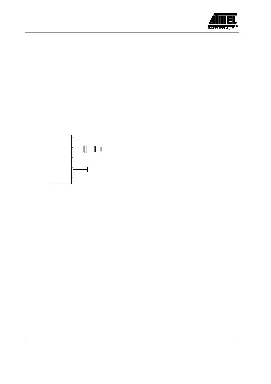
DATA
t DATA_L_max
DATA_min
t
Figure 5. Steady L state limited DATA output pattern
FSK/ASK Demodulator and Data Filter
The signal coming from the RSSI amplifier is converted
into the raw data signal by the ASK/FSK demodulator.
The operating mode of the demodulator is set via the bit
ASK/_FSK in the OPMODE register. Logic `L' sets the
demodulator to FSK, applying `H' to ASK mode.
In ASK mode an automatic threshold control circuit
(ATC) is employed to set the detection reference voltage
to a value where a good signal to noise ratio is achieved.
This circuit also implies the effective suppression of any
kind of in-band noise signals or competing transmitters.
If the S/N (ratio to suppress in-band noise signals) ex-
ceeds about 10 dB the data signal can be detected
properly, but better values are found for many modulation
schemes of the competing transmitter.
The FSK demodulator is intended to be used for an FSK
deviation of 10 kHz
Df
100 kHz. In FSK mode the
data signal can be detected if the S/N (ratio to suppress
inband noise signals) exceeds about 2 dB. This value is
valid for all modulation schemes of a disturber signal.
The output signal of the demodulator is filtered by the
data filter before it is fed into the digital signal processing
circuit. The data filter improves the S/N ratio as its pass-
band can be adopted to the characteristics of the data
signal. The data filter consists of a 1
st
-order highpass and
a 2
nd
-order lowpass filter
The highpass filter cut-off frequency is defined by an
external capacitor connected to Pin CDEM. The cut-off
frequency of the highpass filter is defined by the follow-
ing formula:
fcu_DF
+
1
2
p 30 kW CDEM
In self-polling mode, the data filter must settle very
rapidly to achieve a low current consumption. Therefore,
CDEM cannot be increased to very high values if self-
polling is used. On the other hand CDEM must be large
enough to meet the data filter requirements according to
the data signal. Recommended values for CDEM are
given in the electrical characteristics.
The cut-off frequency of the lowpass filter is defined by
the selected baud-rate range (BR_Range). The
BR_Range is defined in the OPMODE register (refer to
chapter `Configuration of the Receiver'). The BR_Range
must be set in accordance to the used baud-rate.
The T5760/T5761 is designed to operate with data coding
where the DC level of the data signal is 50%. This is valid
for Manchester and Bi-phase coding. If other modulation
schemes are used, the DC level should always remain
within the range of V
DC_min
= 33% and V
DC_max
= 66%.
The sensitivity may be reduced by up to 2 dB in that
condition.
Each BR_Range is also defined by a minimum and a
maximum edge-to-edge time (t
ee_sig
). These limits are
defined in the electrical characteristics. They should not
be exceeded to maintain full sensitivity of the receiver.
Receiving Characteristics
The RF receiver T5760/T5761 can be operated with and
without a SAW front-end filter. In a typical automotive
application, a SAW filter is used to achieve better selec-
tivity and large signal capability. The receiving frequency
response without a SAW front-end filter is illustrated in
figures 6 and 7. This example relates to ASK mode. FSK
mode exhibit similar behavior. The plots are printed rela-
tively to the maximum sensitivity. If a SAW filter is used,
an insertion loss of about 3 dB must be considered, but the
over all selectivity is much better.
When designing the system in terms of receiving band-
width, the LO deviation must be considered as it also
determines the IF center frequency. The total LO devi-
ation is calculated to be the sum of the deviation of the
crystal and the XTO deviation of the T5760/T5761. Low-
cost crystals are specified to be within
±
90 ppm over
tolerance, temperature and aging. The XTO deviation of
the T5760/T5761 is an additional deviation due to the
XTO circuit. This deviation is specified to be
±
30 ppm
worst case for a crystal with CM = 7 fF. If a crystal of
±
90 ppm is used, the total deviation is
±
120 ppm in that
case. Note that the receiving bandwidth and the IF-filter
bandwidth are equivalent in ASK mode but not in FSK
mode.