Rev. 4164E�SCR�02/04
Features
�
80C51 Core
� 12 or 6 Clocks per Instruction (X1 and X2 Modes)
� 256 Bytes Scratchpad RAM
� Dual Data Pointer
� Two 16-bit Timer/Counters: T0 and T1
�
T83C5121 with 16 Kbytes Mask ROM
�
T85C5121 with 16 Kbytes Code RAM
�
T89C5121 with 16 Kbytes Code RAM and 16 Kbytes EEPROM
�
On-chip Expanded RAM (XRAM): 256 Bytes
�
Versatile Host Serial Interface
� Full-duplex Enhanced UART (EUART) with Dedicated Baud Rate Generator (BRG):
Most Standard Speeds up to 230K bits/s at 7.36 MHz
� Output Enable Input
� Multiple Logic Level Shifters Options (1.8V to V
CC
)
� Automatic Level Shifter Option
�
Multi-protocol Smart Card Interface
� Certified with Dedicated Firmware According to ISO 7816, EMV2000, GIE-CB, GSM
11.12V and WHQL Standards
� Asynchronous Protocols T = 0 and T = 1 with Direct and Inverse Modes
� Baud Rate Generator Supporting All ISO7816 Speeds up to D = 32/F = 372
� Parity Error Detection and Indication
� Automatic Character Repetition on Parity Errors
� Programmable Timeout Detection
� Card Clock Stop High or Low for Card Power-down Mode
� Support Synchronous Card with C4 and C8 Programmable Outputs
� Card Detection and Automatic De-activation Sequence
� Step-up/down Converter with Programmable Voltage Output: 5V, 3V (� 8% at
60 mA) and 1.8V (�8% at 20 mA)
� Direct Connection to Smart Card Terminals:
Short Circuit Current Limitation
Logic Level Shifters
4 kV ESD Protection (MIL/STD 833 Class 3)
�
Alternate Card Support with CLK, I/O and RST According to GSM 11.12V Standard
�
2x I/O Ports: 6 I/O Port1 and 8 I/O Port3
�
2x LED Outputs with Programmable Current Sources: 2, 4, or 10 mA
�
Hardware Watchdog
�
Reset Output Includes
� Hardware Watchdog Reset
� Power-on Reset (POR)
� Power-fail Detector (PFD)
�
4-level Priority Interrupt System with 7 Sources
�
7.36 to 16 MHz On-chip Oscillator with Clock Prescaler
�
Absolute CPU Maximal Frequency: 16 MHz in X1 mode, 8MHz in X2 mode
�
Idle and Power-down Modes
�
Voltage Operation: 2.85V to 5.4V
�
Low Power Consumption
� 8 mA Operating Current (at 5.4V and 3.68 MHz)
� 150 mA Maximum Current with Smart Card Power-on (at 16 MHz X1 Mode)
� 30
�
A Maximum Power-down Current at 3.0V (without Smart Card)
� 100
�
A Maximum Power-down Current at 5.4V (without Smart Card)
�
Temperature Range
� Commercial: 0 to +70
�
C Operating Temperature
� Industrial: -40 to +85
�
C Operating Temperature
�
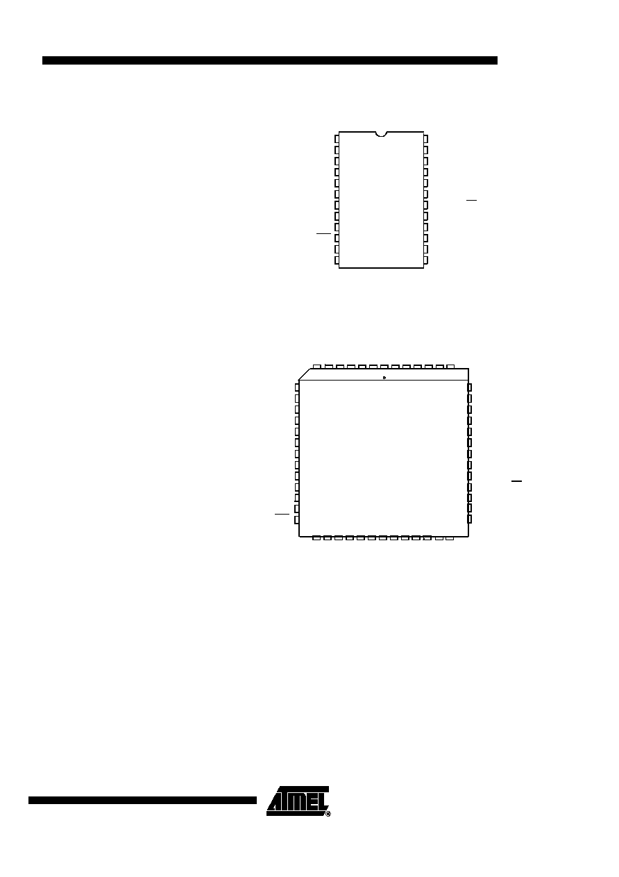
Packages
� SSOP24
� PLCC52
8-bit
Microcontroller
with Multi-
protocol Smart
Card Interface
T83C5121
T85C5121
T89C5121
2
T8xC5121
4164E�SCR�02/04
Description
T8xC5121 is a high performance CMOS ROM/CRAM derivative of the 80C51 CMOS
single chip 8-bit microcontrollers.
T8xC5121 retains the features of the Atmel 80C51 with extended ROM capacity (16
Kbytes), 512 bytes of internal RAM, a 4-level interrupt system, two 16-bit timer/counters
(T0/T1), a full duplex enhanced UART (EUART) with baud rate generator (BRG) and an
on-chip oscillator.
In addition, the T8xC5121 have, a Multi protocol Smart Card Interface, a dual data
pointer, 2 programmable LED current sources (2-4-10 mA) and a hardware Watchdog.
T89C5121 Flash RAM version and T85C5121 Code RAM version can be loaded by In-
System Programming (ISP) software residing in the on-chip ROM from a low-cost exter-
nal serial EEPROM or from R232 interface.
T8xC5121 have 2 software-selectable modes of reduced activity for further reduction in
power consumption.
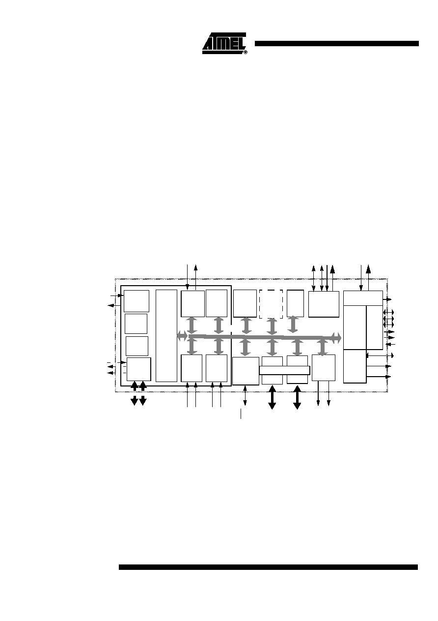
Block Diagram
Figure 1. Block Diagram
Notes:
1. Alternate function of Port 1
2. Alternate function of Port 3
3. Only for the Code RAM version
4. Only for PLCC52
Timer 0
INT
RAM
256 x8
T0
T1
Rx
D
Tx
D
XTAL2
XTAL1
EUART
CPU
Timer 1
INT
1
Ctrl
INT
0
C51
CORE
(2) (2)
(2) (2)
P1
IB-bus
RS
T
VS
S
V
CC
(1):
ROM
Xtal
Osc
XRAM
256
x8
SCIB
CC8
CRST
CPRES
CIO
CC4
CCLK
C
V
CC
6 I/Os
LI
CRST1
CIO1
CCLK1
(2)
(2)
(2)
(4)
16K x8
CRAM
16K x8
(2) (2)
P3
8 I/Os
D
V
CC
Voltage
Reg.
(1)
(1)
(1)
(1)
(1)
(1)
LED
Drive
Direct
LE
D
0
LE
D
1
(2)
(2)
Output
:1-16
Clock
(3)
Prescaler
X2
Watchdog
E
V
CC
CV
S
S
P2
P0
EA
PSEN
ALE
DC/DC
Converter
Level
Shifters
POR
PFD
Alternate
Card
BRG
Parallel I/O Ports
4
T8xC5121
4164E�SCR�02/04
Signals
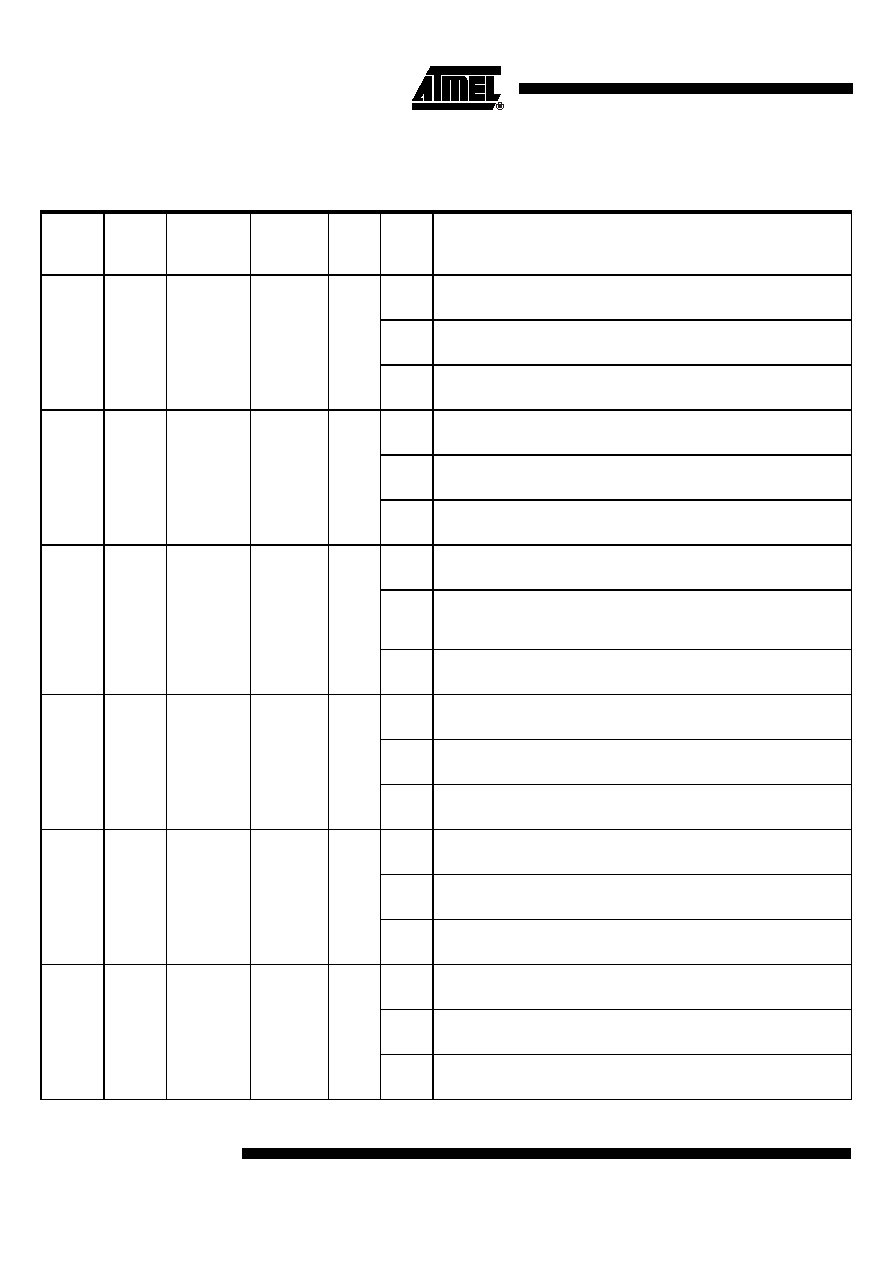
All the T8xC5121 signals are detailed in Table 1.
The port structure is described in Section "Port Structure Description".
Table 1. Ports Description
Port
Signal
Name
Alternate
Internal
Power
Supply
ESD
Type
Description
P1.0
CIO
CV
CC
4 kV
I/O
Smart card interface function
Card I/O.
I/O
Input/Output function
P1.0 is a bi-directional I/O port .
I
Reset configuration
Input .
P1.1
CC8
CV
CC
4 kV
O
Smart card interface function
Card contact 8
O
Output function
P1.1 is a Push-pull port.
I
Reset configuration
Input
P1.2
CPRES
V
CC
4 kV
I
Smart card interface function
Card presence
I/O
Input/Output function
P1.2 is a bi-directional I/O port with internal pull-ups- ( External Pull-up
configuration can be selected).
I
Reset configuration
Input (high level due to internal pull-up)
P1.3
CC4
CV
CC
4 kV
O
Smart card interface function
Card contact 4
O
Output function
P1.3 is a Push-pull port.
I
Reset configuration
Input (high level due to internal pull-up)
P1.4
CCLK
CV
CC
4 kV
O
Smart card interface function
Card clock
I/O
Input/Output function
P1.4 is a a Push-pull port.
O
Reset configuration
Output at low level
P1.5
CRST
CV
CC
4 kV
O
Smart card interface function
Card reset
I/O
Input/Output function
P1.5 is a a Push-pull port.
O
Reset configuration
Output at low level
5
T8xC5121
4164E�SCR�02/04
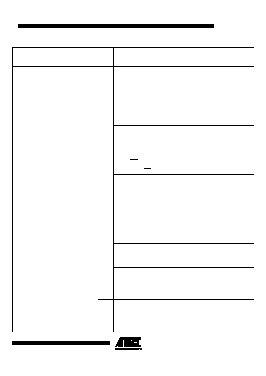
P3.0
RxD
EV
CC
I
UART function
Receive data input
I/O
Input/Output function
P3.0 is a bi-directional I/O port with internal pull-ups.
I
Reset configuration
Input (high level)
P3.1
TxD
EV
CC
O
UART function
Transmit data output
OE active at low or high level depending of PMSOEN bits in SIOCON Reg.
I/O
Input/Output function
P3.1 is a bi-directional I/O port with internal pull-ups.
Z
Reset configuration
High impedance due to PMOS switched OFF
P3.2
INT0
DV
CC
I
External interrupt 0
INT0 input set IE0 in the TCON register. If bit IT0 in this register is set, bits IE0
are set by a falling edge on INT0. If bit IT0 is cleared, bits IE0 is set by a low
level on INT0.
I/O
Input/Output function
P3.2 is a bi-directional I/O port with internal pull-ups.
I
Timer 0: Gate input
INT0 serves as external run control for Timer 0 when
selected in TCON register.
I
Reset configuration
Input (high level)
P3.3
INT1
OE
EV
CC
I
External Interrupt 1
INT1 input set OEIT in ISEL Register, IE1 in the TCON register.
If bit IT1 in this register is set, bits OEIT and IE1 are set by a falling edge on
INT1. If bit IT1 is cleared, bits OEIT and IE1 is set by a low level on INT1
I
UART function
Output enable. A low or high level (depending OELEV bit in
ISEL Register) on this pin disables the PMOS transistors of TxD
(P3.1) and T0 (P3.4). This function can be disabled by software
I/O
Input/Output function
P3.3 is a bi-directional I/O port with internal pull-ups.
I
Timer 1 function: Gate input
INT1 serves as external run control for Timer 1 when
selected in TCON register.
I
Reset configuration
Input (high level)
P3.4
T0
EV
CC
O
UART function
OE active at low or high level depending of PMSOEN
bits in SIOCON Reg.
Table 1. Ports Description (Continued)
Port
Signal
Name
Alternate
Internal
Power
Supply
ESD
Type
Description