
Rev. 4128A≠8051≠04/02
1
Features
∑
80C51 Core Architecture
∑
256 Bytes of On-chip RAM
∑
256 Bytes of On-chip ERAM
≠ 16-KB of On-chip Flash Memory
≠ Data Retention: 10 Years at 85
∞
C
≠ Read/Write Cycle: 10K
∑
2K Bytes of On-chip Flash for Bootloader
∑
2K Bytes of On-chip EEPROM
≠ Read/Write Cycle: 100k
∑
14-sources 4-level Interrupts
∑
Three 16-bit Timers/Counters
∑
Full Duplex UART Compatible 80C51
∑
Maximum Crystal Frequency 40 MHz
≠ In X2 Mode, 20 MHz (CPU core, 40 MHz)
∑
Three or Four Ports: 16 or 20 Digital I/O Lines
∑
Two-channel 16-bit PCA with:
≠ PWM (8-bit)
≠ High-speed Output
≠ Timer and Edge Capture
∑
Double Data Pointer
∑
21-bit WatchDog Timer (7 Programmable Bits)
∑
A 10-bit Resolution Analog to Digital Converter (ADC) with 8 Multiplexed Inputs
∑
Power Saving Modes:
≠ Idle Mode
≠ Power-down Mode
∑
Power Supply: 5V ± 10% (or 3V
(1)
± 10%)
∑
Temperature Range: Industrial (-40
∞
to +85
∞
C)
∑
Packages: SOIC28, PLCC28, VQFP32
Note:
1. Ask for availability
Description
The T89C5115 is a high performance Flash version of the 80C51 single chip 8-bit
microcontrollers. It contains a 16-KB Flash memory block for program and data.
The 16-KB Flash memory can be programmed either in parallel mode or in serial
mode with the ISP capability or with software. The programming voltage is internally
generated from the standard VCC pin.
The T89C5115 retains all features of the 80C52 with 256 bytes of internal RAM, a 7-
source 4-level interrupt controller and three timer/counters. In addition, the T89C5115
has a 10-bit A/D converter, a 2-KB Boot Flash memory, 2-KB EEPROM for data, a
Programmable Counter Array, an ERAM of 256 bytes, a Hardware WatchDog Timer
and a more versatile serial channel that facilitates multiprocessor communication
(EUART). The fully static design of the T89C5115 reduces system power consumption
by bringing the clock frequency down to any value, even DC, without loss of data.
The T89C5115 has two software-selectable modes of reduced activity and an 8 bit
clock prescaler for further reduction in power consumption. In the idle mode the CPU
is frozen while the peripherals and the interrupt system are still operating. In the
power-down mode the RAM is saved and all other functions are inoperative.
The added features of the T89C5115 make it more powerful for applications that need
A/D conversion, pulse width modulation, high speed I/O and counting capabilities
such as industrial control, consumer goods, alarms, motor control, etc. While remain-
ing fully compatible with the 80C52 it offers a superset of this standard microcontroller.
Low Pin Count
8-bit MCU with
A/D Converter
and 16-Kbytes of
Flash Memory
T89C5115

4
T89C5115
4128A≠8051≠04/02
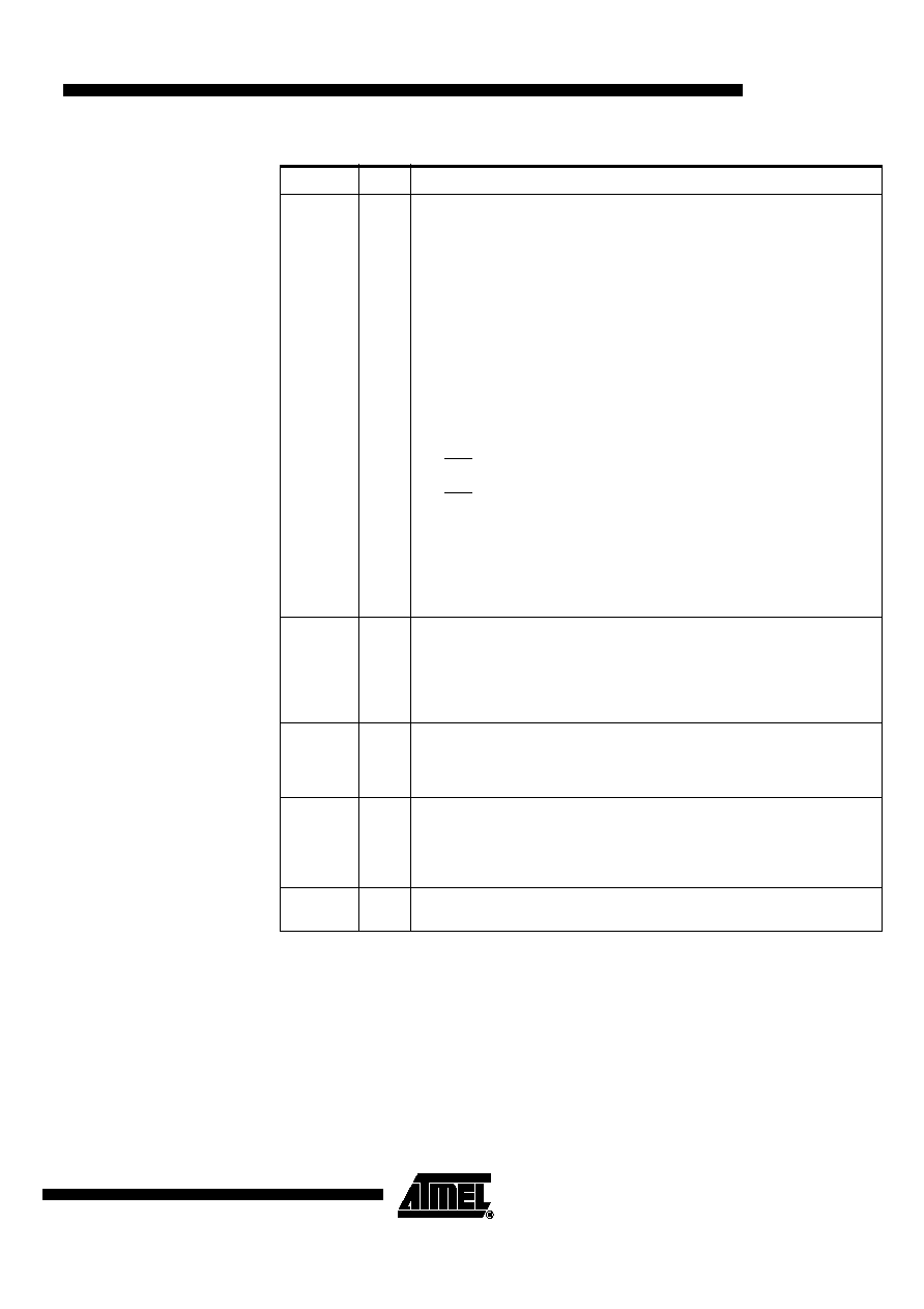
Table 1. Pin Description
Pin Name
Type
Description
VSS
GND
Circuit ground
VCC
Supply Voltage
VAREF
Reference Voltage for ADC
VAVCC
Supply Voltage for ADC
VAGND
Reference Ground for ADC
P1.0:7
I/O
Port 1:
Is an 8-bit bi-directional I/O port with internal pull-ups. Port 1 pins can be used for
digital input/output or as analog inputs for the Analog Digital Converter (ADC). Port 1
pins that have 1's written to them are pulled high by the internal pull-up transistors
and can be used as inputs in this state. As inputs, Port 1 pins that are being pulled
low externally will be the source of current (I
IL
, see section "Electrical Characteristic")
because of the internal pull-ups. Port 1 pins are assigned to be used as analog
inputs via the ADCCF register (in this case the internal pull-ups are disconnected).
As a secondary digital function, port 1 contains the Timer 2 external trigger and clock
input; the PCA external clock input and the PCA module I/O.
P1.0/AN0/T2
Analog input channel 0,
External clock input for Timer/counter2.
P1.1/AN1/T2EX
Analog input channel 1,
Trigger input for Timer/counter2.
P1.2/AN2/ECI
Analog input channel 2,
PCA external clock input.
P1.3/AN3/CEX0
Analog input channel 3,
PCA module 0 Entry of input/PWM output.
P1.4/AN4/CEX1
Analog input channel 4,
PCA module 1 Entry of input/PWM output.
P1.5/AN5
Analog input channel 5,
P1.6/AN6
Analog input channel 6,
P1.7/AN7
Analog input channel 7,
It can drive CMOS inputs without external pull-ups.
P2.0:7
I/O
Port 2:
Is an 2-bit bi-directional I/O port with internal pull-ups. Port 2 pins that have 1's
written to them are pulled high by the internal pull-ups and can be used as inputs in
this state. As inputs, Port 2 pins that are being pulled low externally will be a source
of current (IIL, on the datasheet) because of the internal pull-ups.
In the T89C51CC02 Port 2 can sink or source 5 mA. It can drive CMOS inputs
without external pull-ups.
5
T89C5115
4128A≠8051≠04/02
P3.0:7
I/O
Port 3:
Is an 8-bit bi-directional I/O port with internal pull-ups. Port 3 pins that have 1's
written to them are pulled high by the internal pull-up transistors and can be used as
inputs in this state. As inputs, Port 3 pins that are being pulled low externally will be a
source of current (I
IL
, see section "Electrical Characteristic") because of the internal
pull-ups.
The output latch corresponding to a secondary function must be programmed to one
for that function to operate (except for TxD ). The secondary functions are assigned
to the pins of port 3 as follows:
P3.0/RxD:
Receiver data input (asynchronous) or data input/output (synchronous) of the serial
interface
P3.1/TxD:
Transmitter data output (asynchronous) or clock output (synchronous) of the serial
interface
P3.2/INT0:
External interrupt 0 input/timer 0 gate control input
P3.3/INT1:
External interrupt 1 input/timer 1 gate control input
P3.4/T0:
Timer 0 counter input
P3.5/T1:
Timer 1 counter input
It can drive CMOS inputs without external pull-ups.
P4.0:1
I/O
Port 4:
Is an 2-bit bi-directional I/O port with internal pull-ups. Port 4 pins that have 1's
written to them are pulled high by the internal pull-ups and can be used as inputs in
this state. As inputs, Port 4 pins that are being pulled low externally will be a source
of current (IIL, on the datasheet) because of the internal pull-up transistor.
It can drive CMOS inputs without external pull-ups.
RESET
I/O
Reset:
A high level on this pin during two machine cycles while the oscillator is running
resets the device. An internal pull-down resistor to VSS permits power-on reset
using only an external capacitor to VCC.
XTAL1
I
XTAL1:
Input of the inverting oscillator amplifier and input of the internal clock generator
circuits. To drive the device from an external clock source, XTAL1 should be driven,
while XTAL2 is left unconnected. To operate above a frequency of 16 MHz, a duty
cycle of 50% should be maintained.
XTAL2
O
XTAL2:
Output from the inverting oscillator amplifier.
Table 1. Pin Description (Continued)
Pin Name
Type
Description

