
Rev. 4127D�8051�02/03
1
Features
�
80C51 Core Architecture
�
256 Bytes of On-chip RAM
�
1 KB of On-chip XRAM
�
32 KB of On-chip Flash Memory
� Data Retention: 10 Years at 85�C
Read/Write Cycle: 10K
�
2 KB of On-chip Flash for Bootloader
�
2 KB of On-chip EEPROM
Read/Write Cycle: 100K
�
14-sources 4-level Interrupts
�
Three 16-bit Timers/Counters
�
Full Duplex UART Compatible 80C51
�
Maximum Crystal Frequency 40 MHz, in X2 Mode, 20 MHz (CPU Core, 20 MHz)
�
Five Ports: 32 + 2 Digital I/O Lines
�
Five-channel 16-bit PCA with:
� PWM (8-bit)
� High-speed Output
� Timer and Edge Capture
�
Double Data Pointer
�
21-bit Watchdog Timer (7 Programmable Bits)
�
10-bit Resolution Analog to Digital Converter (ADC) with 8 Multiplexed Inputs
�
On-chip Emulation Logic (Enhanced Hook System)
�
Power Saving Modes:
� Idle Mode
� Power-down Mode
�
Power Supply: 3V to 5.5V
�
Temperature Range: Industrial (-40
�
to +85
�
C)
�
Packages: VQFP44, PLCC44
Description
The T89C51AC2 is a high performance Flash version of the 80C51 single chip 8-bit
microcontrollers. It contains a 32 KB Flash memory block for program and data.
The 32 KB Flash memory can be programmed either in parallel mode or in serial
mode with the ISP capability or with software. The programming voltage is internally
generated from the standard VCC pin.
The T89C51AC2 retains all features of the 80C51 with 256 bytes of internal RAM, a 7-
source 4-level interrupt controller and three timer/counters. In addition, the
T89C51AC2 has a 10-bit A/D converter, a 2 KB Boot Flash memory, 2 KB EEPROM
for data, a Programmable Counter Array, an XRAM of 1024 bytes, a Hardware Watch-
Dog Timer, and a more versatile serial channel that facilitates multiprocessor
communication (EUART). The fully static design of the T89C51AC2 reduces system
power consumption by bringing the clock frequency down to any value, even DC,
without loss of data.
The T89C51AC2 has two software-selectable modes of reduced activity and an 8-bit
clock prescaler for further reduction in power consumption. In the idle mode the CPU
is frozen while the peripherals and the interrupt system are still operating. In the
Power-down mode the RAM is saved and all other functions are inoperative.
The added features of the T89C51AC2 make it more powerful for applications that
need A/D conversion, pulse width modulation, high speed I/O and counting capabili-
ties such as industrial control, consumer goods, alarms, motor control, among others.
While remaining fully compatible with the 80C52, the T8C51AC2 offers a superset of
this standard microcontroller. In X2 mode, a maximum external clock rate of 20 MHz
reaches a 300 ns cycle time.
Enhanced 8-bit
Microcontroller
with 32 KB Flash
Memory
T89C51AC2

2
T89C51AC2
4127D�8051�02/03
Block Diagram
Notes:
1. 8 analog Inputs/8 Digital I/O
2. 2-Bit I/O Port
Timer 0
INT
RAM
256x8
T0
T1
Rx
D
Tx
D
WR
RD
EA
PSEN
ALE
XTAL2
XTAL1
UART
CPU
Timer 1
INT
1
Ctrl
INT
0
C51
CORE
Port 0
P0
Port 1 Port 2 Port 3
Parallel I/O Ports and Ext. Bus
P1
(1)
P2
P3
XRAM
1kx8
IB-bus
PCA
RESET
Watch
Dog
PCA
ECI
Vs
s
Vc
c
Timer 2
T2
EX
T2
Port 4
P4
(2
)
10 bit
ADC
Flash
32kx
8
Boot
loader
2kx8
EE
PROM
2kx8
VA
R
E
F
VA
V
C
C
VAG
N
D
3
T89C51AC2
4127D�8051�02/03
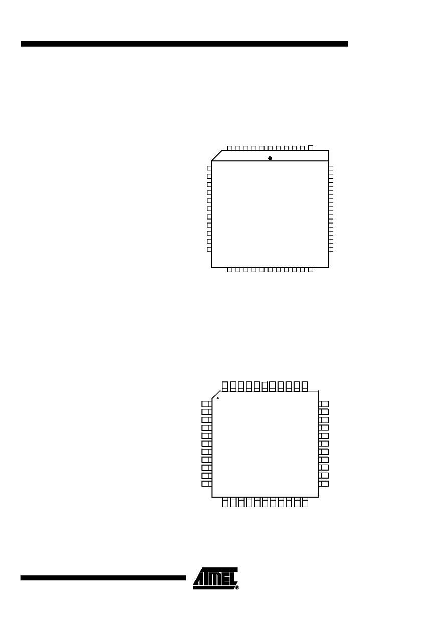
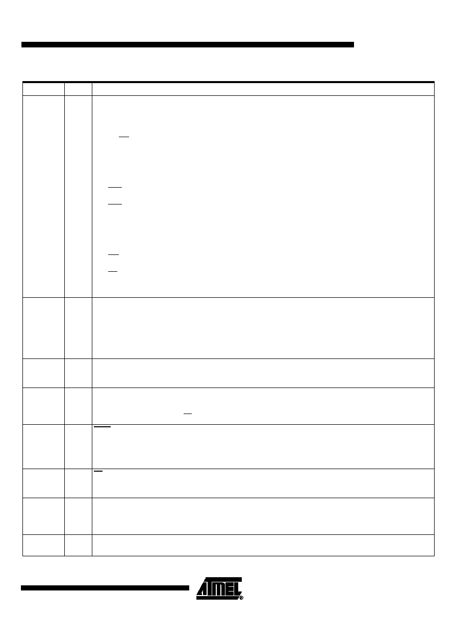
Pin Configuration
PLCC44
P1
.
3
/A
N
3
/C
E
X
0
P1
.
2
/A
N
2
/E
C
I
P1
.
1
/A
N
1
/T
2
E
X
P1.
0
/A
N
0/
T2
VA
R
E
F
VA
G
N
D
RE
S
E
T
VS
S
VC
C
XT
A
L
1
XT
A
L
2
P3.
7
/R
D
P4.
0
P4.
1
P2.
7
/A
15
P2.
6
/A
14
P2.
5
/A
13
P2.
4
/A
12
P2.
3
/A
11
P2.
2
/A
10
P2.
1
/A
9
P3
.6/
W
R
39
38
37
36
35
34
33
32
29
30
31
7
8
9
10
11
12
13
14
17
16
15
18
19
20
21
22
23
24
25
26
27
28
6
5
4
3
2
44
43
42
41
40
ALE
PSEN
P0.7/AD7
P0.6/AD6
P0.5/AD5
P0.2/AD2
P0.3/AD3
P0.4/AD4
P0.1/AD1
P0.0/AD0
P2.0/A8
P1.4/AN4/CEX1
P1.5/AN5/CEX2
P1.6/AN6/CEX3
P1.7/AN7/CEX4
EA
P3.0/RxD
P3.1/TxD
P3.2/INT0
P3.3/INT1
P3.4/T0
P3.5/T1
1
43 42 41 40 39
44
38 37 36 35 34
12 13
17
16
15
14
20
19
18
21 22
33
32
31
30
29
28
27
26
25
24
23
VQFP44
1
2
3
4
5
6
7
8
9
10
11
P1.4/AN4/CEX1
P1.5/AN5/CEX2
P1.6/AN6/CEX3
P1.7/AN7/CEX4
EA
P3.0/RxD
P3.1/TxD
P3.2/INT0
P3.3/INT1
P3.4/T0
P3.5/T1
ALE
PSEN
P0.7/AD7
P0.6/AD6
P0.5/AD5
P0.2 /AD2
P0.3 /AD3
P0.4 /AD4
P0.1 /AD1
P0.0 /AD0
P2.0/A8
P
1
.
3
/AN3/CE
X
0
P
1
.
2
/AN2/E
CI
P
1
.
1
/AN1/T
2E
X
P
1
.
0
/AN 0/
T2
V
ARE
F
VA
GN
D
RE
S
E
T
VS
S
VC
C
XT
A
L
1
XT
A
L
2
P3.
7
/R
D
P4.
0
P4.
1
P2.
7
/A
1
5
P2.
6
/A
1
4
P2.
5
/A
1
3
P2.
4
/A
1
2
P2.
3
/A
1
1
P2.
2
/A
1
0
P2.
1
/A
9
P
3
.6
/W
R

4
T89C51AC2
4127D�8051�02/03
Table 1. Pin Description
Pin Name
Type
Description
VSS
GND
Circuit ground
VCC
Supply Voltage
VAREF
Reference Voltage for ADC
VAGND
Reference Ground for ADC
P0.0:7
I/O
Port 0:
Is an 8-bit open drain bi-directional I/O port. Port 0 pins that have 1's written to them float, and in this state can be used as
high-impedance inputs. Port 0 is also the multiplexed low-order address and data bus during accesses to external Program
and Data Memory. In this application it uses strong internal pull-ups when emitting 1's.
Port 0 also outputs the code Bytes during program validation. External pull-ups are required during program verification.
P1.0:7
I/O
Port 1:
Is an 8-bit bi-directional I/O port with internal pull-ups. Port 1 pins can be used for digital input/output or as analog inputs for
the Analog Digital Converter (ADC). Port 1 pins that have 1's written to them are pulled high by the internal pull-up transistors
and can be used as inputs in this state. As inputs, Port 1 pins that are being pulled low externally will be the source of current
(I
IL
, see section "Electrical Characteristic") because of the internal pull-ups. Port 1 pins are assigned to be used as analog
inputs via the ADCCF register (in this case the internal pull-ups are disconnected).
As a secondary digital function, port 1 contains the Timer 2 external trigger and clock input; the PCA external clock input and
the PCA module I/O.
P1.0/AN0/T2
Analog input channel 0,
External clock input for Timer/counter2.
P1.1/AN1/T2EX
Analog input channel 1,
Trigger input for Timer/counter2.
P1.2/AN2/ECI
Analog input channel 2,
PCA external clock input.
P1.3/AN3/CEX0
Analog input channel 3,
PCA module 0 Entry of input/PWM output.
P1.4/AN4/CEX1
Analog input channel 4,
PCA module 1 Entry of input/PWM output.
P1.5/AN5/CEX2
Analog input channel 5,
PCA module 2 Entry of input/PWM output.
P1.6/AN6/CEX3
Analog input channel 6,
PCA module 3 Entry of input/PWM output.
P1.7/AN7/CEX4
Analog input channel 7,
PCA module 4 Entry ot input/PWM output.
Port 1 receives the low-order address byte during EPROM programming and program verification.
It can drive CMOS inputs without external pull-ups.
P2.0:7
I/O
Port 2:
Is an 8-bit bi-directional I/O port with internal pull-ups. Port 2 pins that have 1's written to them are pulled high by the internal
pull-ups and can be used as inputs in this state. As inputs, Port 2 pins that are being pulled low externally will be a source of
current (I
IL
, see section "Electrical Characteristic") because of the internal pull-ups. Port 2 emits the high-order address byte
during accesses to the external Program Memory and during accesses to external Data Memory that uses 16-bit addresses
(MOVX @DPTR). In this application, it uses strong internal pull-ups when emitting 1's. During accesses to external Data
Memory that use 8 bit addresses (MOVX @Ri), Port 2 transmits the contents of the P2 special function register.
It also receives high-order addresses and control signals during program validation.
It can drive CMOS inputs without external pull-ups.
5
T89C51AC2
4127D�8051�02/03
P3.0:7
I/O
Port 3:
Is an 8-bit bi-directional I/O port with internal pull-ups. Port 3 pins that have 1's written to them are pulled high by the internal
pull-up transistors and can be used as inputs in this state. As inputs, Port 3 pins that are being pulled low externally will be a
source of current (I
IL
, see section "Electrical Characteristic") because of the internal pull-ups.
The output latch corresponding to a secondary function must be programmed to one for that function to operate (except for
TxD and WR). The secondary functions are assigned to the pins of port 3 as follows:
P3.0/RxD:
Receiver data input (asynchronous) or data input/output (synchronous) of the serial interface
P3.1/TxD:
Transmitter data output (asynchronous) or clock output (synchronous) of the serial interface
P3.2/INT0:
External interrupt 0 input/timer 0 gate control input
P3.3/INT1:
External interrupt 1 input/timer 1 gate control input
P3.4/T0:
Timer 0 counter input
P3.5/T1:
Timer 1 counter input
P3.6/WR:
External Data Memory write strobe; latches the data byte from port 0 into the external data memory
P3.7/RD:
External Data Memory read strobe; Enables the external data memory.
It can drive CMOS inputs without external pull-ups.
P4.0:1
I/O
Port 4:
Is an 2-bit bi-directional I/O port with internal pull-ups. Port 4 pins that have 1's written to them are pulled high by the internal
pull-ups and can be used as inputs in this state. As inputs, Port 4 pins that are being pulled low externally will be a source of
current (IIL, on the datasheet) because of the internal pull-up transistor.
P4.0
P4.1:
It can drive CMOS inputs without external pull-ups.
RESET
I/O
Reset:
A high level on this pin during two machine cycles while the oscillator is running resets the device. An internal pull-down
resistor to VSS permits power-on reset using only an external capacitor to VCC.
ALE
O
ALE:
An Address Latch Enable output for latching the low byte of the address during accesses to the external memory. The ALE is
activated every 1/6 oscillator periods (1/3 in X2 mode) except during an external data memory access. When instructions are
executed from an internal Flash (EA = 1), ALE generation can be disabled by the software.
PSEN
O
PSEN:
The Program Store Enable output is a control signal that enables the external program memory of the bus during external
fetch operations. It is activated twice each machine cycle during fetches from the external program memory. However, when
executing from of the external program memory two activations of PSEN are skipped during each access to the external Data
memory. The PSEN is not activated for internal fetches.
EA
I
EA:
When External Access is held at the high level, instructions are fetched from the internal Flash when the program counter is
less then 8000H. When held at the low level,T89C51AC2 fetches all instructions from the external program memory
.
XTAL1
I
XTAL1:
Input of the inverting oscillator amplifier and input of the internal clock generator circuits.
To drive the device from an external clock source, XTAL1 should be driven, while XTAL2 is left unconnected. To operate
above a frequency of 16 MHz, a duty cycle of 50% should be maintained.
XTAL2
O
XTAL2:
Output from the inverting oscillator amplifier.
Table 1. Pin Description (Continued)
Pin Name
Type
Description