Rev. F - 15 February, 2001
1
T89C51RD2
0 to 40MHz Flash Programmable 8-bit Microcontroller
1. Description
ATMEL Wireless and Microcontrollers T89C51RD2 is
high performance CMOS Flash version of the 80C51
CMOS single chip 8-bit microcontroller. It contains a
64 Kbytes Flash memory block for program and for data.
The 64 Kbytes Flash memory can be programmed either
in parallel mode or in serial mode with the ISP capability
or with software. The programming voltage is internally
generated from the standard V
CC
pin.
The T89C51RD2 retains all features of the ATMEL
Wireless and Microcontrollers 80C52 with 256 bytes of
internal RAM, a 7-source 4-level interrupt controller and
three timer/counters.
In addition, the T89C51RD2 has a Programmable
Counter Array, an XRAM of 1024 bytes, an EEPROM
of 2048 bytes, a Hardware Watchdog Timer, a more
versatile serial channel that facilitates multiprocessor
communication (EUART) and a speed improvement
mechanism (X2 mode). Pinout is either the standard 40/
44 pins of the C52 or an extended version with 6 ports
in a 64/68 pins package.
The fully static design of the T89C51RD2 allows to
reduce system power consumption by bringing the clock
frequency down to any value, even DC, without loss of
data.
The T89C51RD2 has 2 software-selectable modes of
reduced
activity
for
further
reduction
in
power
consumption. In the idle mode the CPU is frozen while
the peripherals and the interrupt system are still
operating. In the power-down mode the RAM is saved
and all other functions are inoperative.
The added features of the T89C51RD2 makes it more
powerful for applications that need
pulse width
modulation, high speed I/O and counting capabilities
such as alarms, motor control, corded phones, smart card
readers.
2. Features
�
80C52 Compatible
�
8051 pin and instruction compatible
�
Four 8-bit I/O ports (or 6 in 64/68 pins packages)
�
Three 16-bit timer/counters
�
256 bytes scratch pad RAM
�
7 Interrupt sources with 4 priority levels
�
ISP (In System Programming) using standard V
CC
power supply.
�
Boot
FLASH
contains
low
level
FLASH
programming routines and a default serial loader
�
High-Speed Architecture
�
40 MHz in standard mode
�
20 MHz in X2 mode (6 clocks/machine cycle)
�
64K bytes on-chip Flash program / data Memory
�
Byte and page (128 bytes) erase and write
�
10k write cycles
�
On-chip 1024 bytes expanded RAM (XRAM)
�
Software selectable size (0, 256, 512, 768, 1024
bytes)
�
768 bytes selected at reset for T87C51RD2
compatibility
�
Dual Data Pointer
�
Variable length MOVX for slow RAM/peripherals
�
Improved X2 mode with independant selection for
CPU and each peripheral
�
2 k bytes EEPROM block for data storage
�
100K Write cycle
�
Programmable Counter Array with:
�
High Speed Output,
�
Compare / Capture,
�
Pulse Width Modulator,
�
Watchdog Timer Capabilities
�
Asynchronous port reset
�
Full duplex Enhanced UART
�
Low EMI (inhibit ALE)
�
Hardware Watchdog Timer (One-time enabled with
Reset-Out)
�
Power control modes:
�
Idle Mode.
�
Power-down mode.
2
Rev. F - 15 February, 2001
T89C51RD2
�
Power supply:
- M version: Commercial and industrial
4.5V to 5.5V : 40MHz X1 Mode, 20MHz X2 Mode
3V to 5.5V : 33MHz X1 Mode, 16 MHz X2 Mode
- L version: Commercial and industrial
2.7V to 3.6V : 25MHz X1 Mode, 12MHz X2 Mode
�
Temperature ranges: Commercial (0 to +70
�
C) and industrial (-40 to +85
�
C).
�
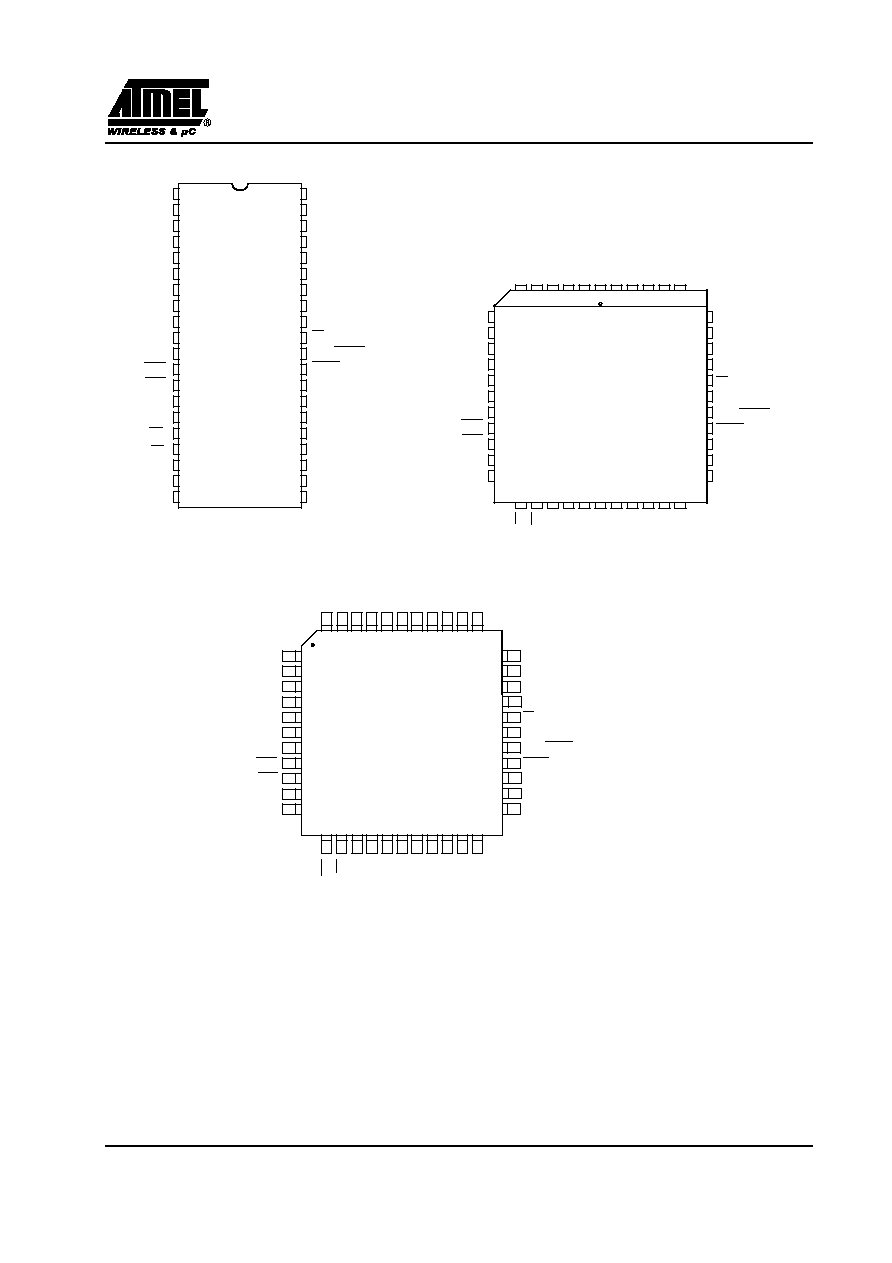
Packages: PDIL40, PLCC44, VQFP44, PLCC68, VQFP64
Table 1. Memory Size
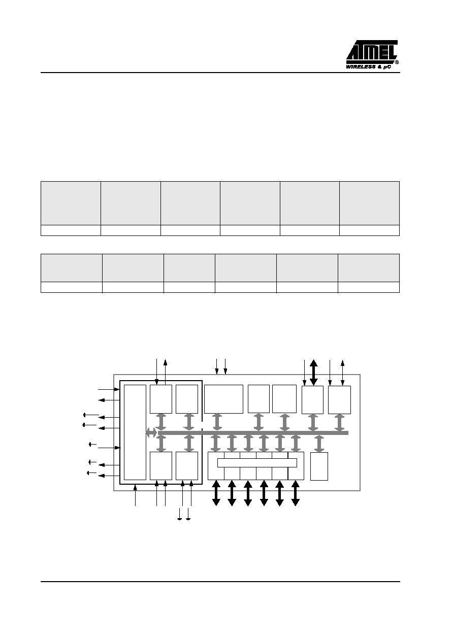
3. Block Diagram
PDIL40
PLCC44
VQFP44 1.4
Flash (bytes)
EEPROM (bytes)
XRAM (bytes)
TOTAL RAM
(bytes)
I/O
T89C51RD2
64k
2k
1024
1280
32
PLCC68
VQFP64 1.4
Flash (bytes)
EEPROM
(bytes)
XRAM (bytes)
TOTAL RAM
(bytes)
I/O
T89C51RD2
64k
2k
1024
1280
48
Timer 0
INT
RAM
256x8
T0
T1
RxD
TxD
WR
RD
EA
PSEN
ALE/
XTAL2
XTAL1
EUART
CPU
Timer 1
INT1
Ctrl
INT0
(3)
(3)
C51
CORE
(3) (3)
(3) (3)
Port 0
P0
Port 1 Port 2 Port 3
Parallel I/O Ports & Ext. Bus
P1
P2
P3
XRAM
1Kx8
IB-bus
PCA
RESET
PROG
Watch
Dog
PCA
ECI
Vss
V
CC
(3)
(3)
(1)
(1): Alternate function of Port 1
(3): Alternate function of Port 3
(1)
Timer2
T2EX
T2
(1)
(1)
Port 5
Port 4
P5
P4
(2): Only available on high pin count packages
(2)
(2)
Flash
64Kx8
EEPROM
2Kx8

Rev. F - 15 February, 2001
3
T89C51RD2
4. SFR Mapping
The Special Function Registers (SFRs) of the T89C51RD2 fall into the following categories:
�
C51 core registers: ACC, B, DPH, DPL, PSW, SP, AUXR1
�
I/O port registers: P0, P1, P2, P3, P4, P5
�
Timer registers: T2CON, T2MOD, TCON, TH0, TH1, TH2, TMOD, TL0, TL1, TL2, RCAP2L, RCAP2H
�
Serial I/O port registers: SADDR, SADEN, SBUF, SCON
�
Power and clock control registers: PCON
�
Hardware Watchdog Timer register: WDTRST, WDTPRG
�
Interrupt system registers: IE, IP, IPH
�
Flash and EEPROM registers: FCON, EECON, EETIM
�
Others: AUXR, AUXR1, CKCON
Table below shows all SFRs with their address and their reset value.
Bit
address-
able
Non Bit addressable
0/8
1/9
2/A
3/B
4/C
5/D
6/E
7/F
F8h
CH
0000 0000
CCAP0H
XXXX XXXX
CCAP1H
XXXX XXXX
CCAPL2H
XXXX XXXX
CCAPL3H
XXXX XXXX
CCAPL4H
XXXX XXXX
FFh
F0h
B
0000 0000
F7h
E8h
P5
1111 1111
CL
0000 0000
CCAP0L
XXXX XXXX
CCAP1L
XXXX XXXX
CCAPL2L
XXXX XXXX
CCAPL3L
XXXX XXXX
CCAPL4L
XXXX XXXX
EFh
E0h
ACC
0000 0000
E7h
D8h
CCON
00X0 0000
CMOD
00XX X000
CCAPM0
X000 0000
CCAPM1
X000 0000
CCAPM2
X000 0000
CCAPM3
X000 0000
CCAPM4
X000 0000
DFh
D0h
PSW
0000 0000
FCON
XXXX 0000
EECON
XXXX XX00
EETIM
0000 0000
D7h
C8h
T2CON
0000 0000
T2MOD
XXXX XX00
RCAP2L
0000 0000
RCAP2H
0000 0000
TL2
0000 0000
TH2
0000 0000
CFh
C0h
P4
1111 1111
P5
1111 1111
C7h
B8h
IP
X000 000
SADEN
0000 0000
BFh
B0h
P3
1111 1111
IPH
X000 0000
B7h
A8h
IE
0000 0000
SADDR
0000 0000
AFh
A0h
P2
1111 1111
AUXR1
XXXX 00X0
WDTRST
XXXX XXXX
WDTPRG
XXXX X000
A7h
98h
SCON
0000 0000
SBUF
XXXX XXXX
9Fh
90h
P1
1111 1111
97h
88h
TCON
0000 0000
TMOD
0000 0000
TL0
0000 0000
TL1
0000 0000
TH0
0000 0000
TH1
0000 0000
AUXR
XX0X 1000
CKCON
X000 0000
8Fh
80h
P0
1111 1111
SP
0000 0111
DPL
0000 0000
DPH
0000 0000
PCON
00X1 0000
87h
0/8
1/9
2/A
3/B
4/C
5/D
6/E
7/F