U2510B
Rev. A3, 23-Feb-01
1 (15)
All-Band AM/FM Receiver and Audio Amplifier
Description
The U2510B is an integrated bipolar one-chip AM/FM
radio circuit. It contains an FM front end with
preamplifier, FM IF and demodulator, a complete AM
receiver, an AF amplifier and a mode switch for AM, FM
and tape. This circuit is designed for clock radios and
portable radio-cassette recorders.
Features
D Superior FM strong signal behavior by using RF AGC
D Soft mute and HCC for decreasing interstation noise
in FM mode
D Excellent AFC performance (level controlled, both
polarities available)
D Level indicator (LED drive) for AM and FM
D DC mode control: AM, FM and tape
D Wide supply-voltage range and low quiescent current
D High AF output power: 1 W
D Electronic volume control
D Electronic AF bandwidth control (treble and high cut)
D Output stage for headphone and speaker drive
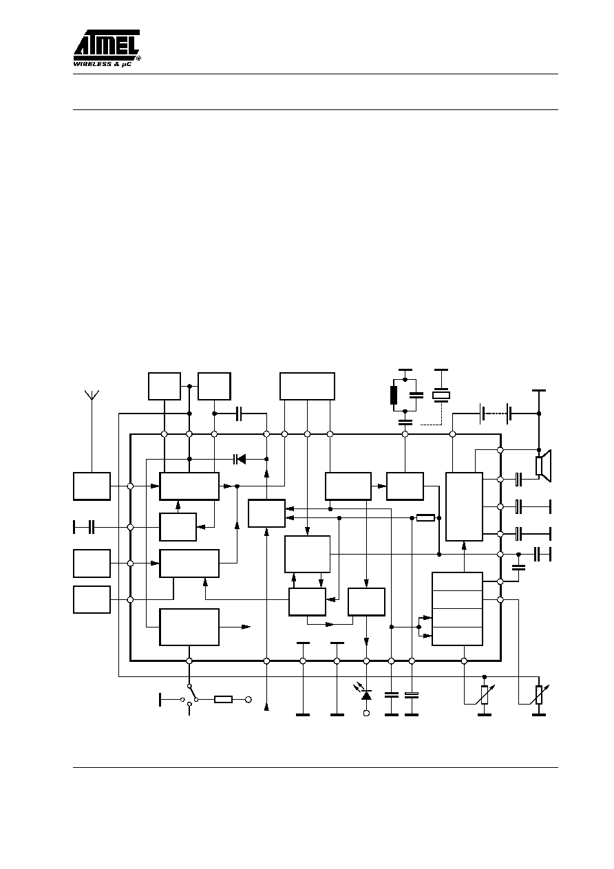
Block Diagram
FM
front end
9
AM
front end
FM
AGC
12
13912
Voltage stab.
and
mode control
AM/FM
AFC
control
AM IF
amp. and
detect.
AM
AGC
Level
indic.
FM IF
amp.
FM
discr.
15
Power
amp.
28
AF preamp.
Volume
Mute
HCC
8
7
6
AFC
14
16
27
3
25
23
24
4
FM osc.
tank
FM RF
tank
IF BPE
2
26
(Replaceable)
FM RF
BPE
AM
ant.
AM osc.
tank
11
10
5
AGC
FM ant.
21
13
20
19
1
22
18
V
S
Treble
Vol
V
S
LED
AFC mode
Tape
AM
FM
V
S
IF
AGC
IF
RF AGC
V
Ref
S
2
Figure 1. Block diagram

U2510B
Rev. A3, 23-Feb-01
2 (15)
Order Information
Extended Type Number
Package
Remarks
U2510B-M
SDIP28
U2510B-M__T
SDIP28
V
S
< 6 V supply voltage
Pin Description
1
2
3
4
5
6
7
8
10
9
27
22
21
20
18
19
17
12
11
28
25
26
23
24
FM-AFC
FMOsc
V
Ref
FMtank
AMtank
FM-AGC
Vol ctrl in
AMOsc
FMin
CF
FM-discr
Mute
AM/FM detect
V
AGC/AFC
AFC switch
IF-GND
LED drive
V
Treble in
Ripple in
AFin
FM-IFin
V
S
AFout
AF-GND
16
15
14
13
14812
FE-GND
AM/FM
IFout
AM-IFin
Mode ctrl
switch
Figure 2. Pinning
Pin
Symbol
Function
1
Mute
Mute voltage output, time constant (C
23
),
mute depth and threshold adjustable by load
resistance (R
3
)
2
FM-discr
FM discriminator filter connection, ceramic
resonator or equivalent LC-circuit
3
CF
Audio negative feedback input. Blocking
capacitor (C
8
) determines the audio amplifiers
low-end cut-off frequency
4
Vol ctrl in
Input for volume control voltage
Pin
Symbol
Function
5
AMOsc
AM oscillator tank circuit input, recommended
load impedance approximately 2.5 k
W
6
FM≠AFC
AFC diode connection, coupling capacitor
(C
19
) determines the AFC characteristic
(holding range and slope)
7
FMOsc
FM oscillator tank circuit input, recommended
load impedance approximately 3 k
W
8
V
Ref
Regulated voltage output (2.4 V)
9
FMtank
FM RF tank circuit connection, recommended
load impedance approximately 3 k
W
10
AMtank
AM RF tank circuit connection, recommended
load impedance approximately 20 k
W
11
FM-AGC
FM AGC voltage output, time constant (C
20
).
Loading this pin by a resistor (to GND) will
increase the FM AGC threshold, grounding
this pin will switch off the FM AGC function
12
FMin
FM RF input (common-base preamplifier
transistor), recommended (RF) source
impedance approximately 100
W
13
FE-GND
FM front-end ground
14
AM/FM
IFout
AM/FM IF output
(collector output of the IF preamplifier)
15
Mode ctrl
switch
Mode control input:
Pin
| Function
open
| FM
Ground
| AM
V
S
(R
4
= 10 k
W) | Tape
16
AM-IFin
AM IF input, input impedance = 3.1 k
W
17
FM-IFin
FM IF input, input impedance = 330
W
18
V
Treble in
Treble control voltage input
19
LED drive
Level indicator output
(open-collector output, LED drive)
20
IF-GND
IF ground
21
AFC switch
AFC function control input:
Pin
| Function
open
| AFC off
Ground
| f
OSC
> f
in
V
S
| f
OSC
< f
in
22
V
AGC/AFC
AGC/AFC voltage, time constant adjust (C
10
),
input impedance approximately 42 k
W
23
AM/FM
detect
AM/FM detector output, the load capacitor
(C
11
) in conjunction with the detector output
resistance (7.5 k
W) determines the (FM)
deemphasis as well as the (modulation)
frequency response of the AM detector
24
AFin
Audio amplifier input, input resistance
approximately 100 k
W, coupling capacitor
(C
9
) determines the low frequency response
25
Ripple in
Ripple filter connection. Load capacitance
(C
12
) determines the frequency response of the
supply-voltage ripple rejection
26
V
S
Supply voltage input
27
AFout
Audio amplifier output
28
AF-GND
Ground of the audio power stage
U2510B
Rev. A3, 23-Feb-01
4 (15)
Absolute Maximum Ratings
Parameters
Symbol
Value
Unit
Supply voltage
V
S
13
V
Power dissipation
P
tot
900
mW
Ambient temperature range
T
amb
≠20 to +75
∞
C
Electrical Characteristics
V
S
= 6 V, T
amb
= 25
∞
C, test circuit (figure 16), unless otherwise specified
Parameters
Test Conditions / Pins
Symbol
Min.
Typ.
Max.
Unit
Supply voltage range
V
S
2.5
9 *
V
Oscillator stop voltage
V
S
2.2
V
Operating temperature range
T
≠20
+75
∞
C
Supply quiescent current
V
i1
= V
i2
= V
4
= 0;
AM
(S
2
= AM)
FM
(S
2
= FM)
TAPE (S
2
= Tape)
I
S
I
S
I
S
4.0
6.5
2.2
mA
mA
mA
Regulated voltage
Pin 8
V
Ref
2.4
V
Audio amplifier V
i3
(Pin 24), test point: V
o
(Pin 27) f = 1 kHz
AF measuring range: 30 Hz to 20 kHz, S
2
= Tape, S
4
= A, S
5
= A
Input resistance
Pin 24
R
j
100
k
W
Closed loop voltage gain
GV
af1
= 20 log (V
o
/V
i3
)
V
i3
= 10 mV
GV
af1
40
dB
Output voltage
V
i3
= 100 mV, S
4
= B
V
o
0.7
3
mV
High≠end cut-off frequency
f
c
(≠3 dB)
S
5
= B
f
c
f
c
13
0.8
kHz
kHz
Supply-voltage rejection ratio
SVRR = 20 log (V
hum
/V
o
)
V
hum
= 200 mV,
f
hum
= 200 Hz, S
4
= B
SVRR
32
dB
Noise voltage
S
4
= B, V
i3
= 0
V
n
300
1000
mV
AF output power
THD = 10 %, R
L
= 8
W
V
S
= 4.5 V
V
S
= 6.0 V
V
S
= 9.0 V
P
o
P
o
P
o
400
225
420
1000
mW
mW
mW
Distortion
P
o
= 50 mW, R
L
= 8
W
d
0.6
%
FM section, V
i2
= 60 dB
mV, f
i2
= 98 MHz, f
m
= 1 kHz, dev. =
" 22.5 kHz, f
iIF
= 10.7 MHz,
AF measuring range: 300 Hz to 20 kHz, S
2
= FM, S
1
= A, S
6
= B, test point: V
D
(Pin 23)
FM front-end voltage gain
GV
FM
= 20 log (V
iIF
/ V
i2
)
S
1
= B, V
i2
= 40 db
mV
GV
FM
30
dB
Recovered audio voltage
Pin 23
VD
af
85
mV
Detector output resistance
Pin 23
R
Do
7.5
k
W
Detector output distortion
dev. =
" 75 kHz
V
i2
= 60 dB
mV
V
i2
= 105 dB
mV
THD
THD
0.5
0.8
%
%
*
U2510B-M__T: max. 6 V

U2510B
Rev. A3, 23-Feb-01
5 (15)
Electrical Characteristics (continued)
V
S
= 6 V, T
amb
= 25
∞
C, test circuit (figure 16), unless otherwise specified
Parameters
Test Conditions / Pins
Symbol
Min.
Typ.
Max.
Unit
AM rejection ratio
m = 30%
AM
RR
25
dB
RF sensitivity
(S+N)/N = 26 dB
(S+N)/N = 46 dB
V
i2
V
i2
9
22
dB
mV
dB
mV
Limiting threshold (-3 dB)
V
i2
3
dB
mV
Mute voltage
Test point: Mute
V
i2
= 0
V
i2
= 60 dB
mV
V
mute
V
mute
1.8
0.4
V
V
Mute depth
Referred to V
0
at V
i2
= 0
S
6
= A
S
6
= C
MD
MD
26
20
dB
dB
AFC holding range
f
OSC
> f
in
, S
3
= A, S
6
= A
V
i2
x
10 dB
mV
V
i2
= 20 dB
mV
V
i2
= 80 dB
mV
FHR
FHR
FHR
no AFC
" 180
" 220
kHz
kHz
LED current
I
LED
5.5
mA
Oscillator voltage
eZ
load
= 2.5 k
W Pin 7
V
OSC
180
mV
AM section V
i1
= 60 dB
mV, f
i1
= 1.6 MHz, f
m
= 1 kHz, m = 30%, f
iIF
= 455 kHz,
AF measuring range: 300 Hz to 20 kHz, (S
2
= AM, S
1
= B, test point: V
D
)
AM front end voltage gain
GV
AM
= 20 log (V
iIF
/V
i1
)
V
i1
= 20 dB
mV, S
1
= A
GV
AM
25
dB
Recovered audio voltage
V
D af1
70
mV
Detector output resistance
Pin 23
R
Do
7.5
k
W
Detector output distortion
V
i1
= 60 dB
mV
V
i1
= 105 dB
mV
THD
THD
1
3
%
%
RF sensitivity
(S+N)/N= 10 dB
(S+N)/N= 26 dB
(S+N)/N= 46 dB
V
i1
V
i1
V
i1
0
16
35
dB
mV
dB
mV
dB
mV
AGC figure of merit referred
to V
D af
V
i1
= 105 dB
mV, voltage
drop (V
D af
) = ≠10 dB
FOM
100
dB
IF input resistance
Pin 16
Z
i
3.1
k
W
LED current
I
LED
5.5
mA
Oscillator voltage
Pin 5
V
OSC
160
mV