U2730B-N
Preliminary Information
Rev. A2, 06-Oct-00
1 (14)
Improved L-Band Down-Converter for DAB Receivers
Description
The U2730B-N is a monolithically integrated L-band
down-converter circuit fabricated in Atmel Wireless &
Microcontrollers' advanced UHF5S technology. This IC
is an improved version of the U2730B-B and covers all
functions of an L-band downconverter in a DAB receiver.
The device includes a gain controlled amplifier, a gain
controlled mixer, an output buffer, a gain control block,
a power save function for the analog part, an L-band oscil-
lator and a complete frequency syntheziser unit. The
frequency syntheziser block consists of a reference oscil-
lator/ buffer, a reference divider, a RF divider, a tristate
phase detector, a loop filter amplifier, a lock detector, a
programmable charge pump, a test interface and a control
interface.
Electrostatic sensitive device.
Observe precautions for handling.
Features
D Supply voltage: 8.5 V
D RF frequency range: 1400 MHz to 1550 MHz
D IF frequency range: 150 MHz to 250 MHz
D Enhanced IM3 rejection
D Overall gain control range: typ. 30 dB
D DSB noise figure: 9.5 dB
D Gain-controlled amplifier and L-band mixer
D Power-down function for the analog part
D On-chip gain-control circuitry
D On-chip VCO, typical frequency 1261.568 MHz
D Internal VCO can be overdriven by an external LO
D On-chip frequency synthesizer
≠
Fixed LO divider factor: 2464
≠
Nine reference divider factors selectable: 32, 33, 35, 36,
48, 49, 63, 64, 65
≠
A reference oscillator (can be overdriven by an external
reference signal
≠
Tristate phase detector with programmable charge pump
≠
De-activation of tuning output programmable
≠
Lock-status indication
≠
Test interface
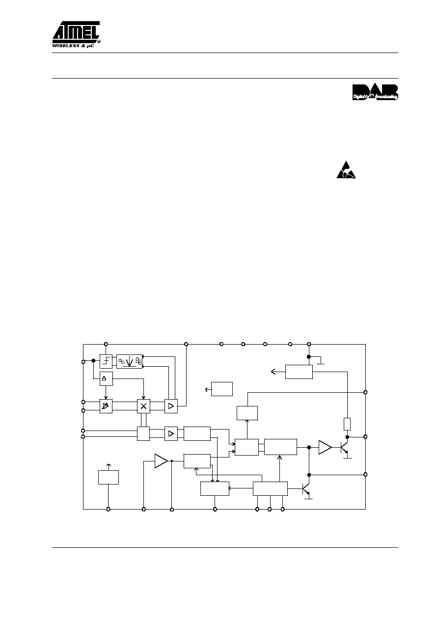
Block Diagram
Power
down
Power save
RF counter
: 2464
Reference
counter
: Nref
Tristate
phase
detector
Charge
pump (200u/
300u)
Control
interface
20k
Test
interface
Lock
detector
Voltage
stabilizer
VCO
U
for frequency synthesizer
Band-
gap
Analog
part
PSM
TI
CI SI1 SI2
PD
CD
GND
PLCK
OSCB
NRF
RF
AGC
18
26
25
TH
17
IF
19
9
VCC2
20
VCC3
3
VCC1
28
VCC4
6, 7, 8, 21,
22, 23, 24
14
12
13
2
27
10
11
OSCE
16
15
1
TANK
VREF
5
4
Internal 5 V supply voltage
(analog part)
Figure 1. Block diagram
U2730B-N
Rev. A2, 06-Oct-00
Preliminary Information
2 (14)
Ordering Information
Extended Type Number
Package
Remarks
U2730B-NFS
SSO28
Tube
U2730B-NFSG1
SSO28
Taped and reeled according to IEC 286≠3
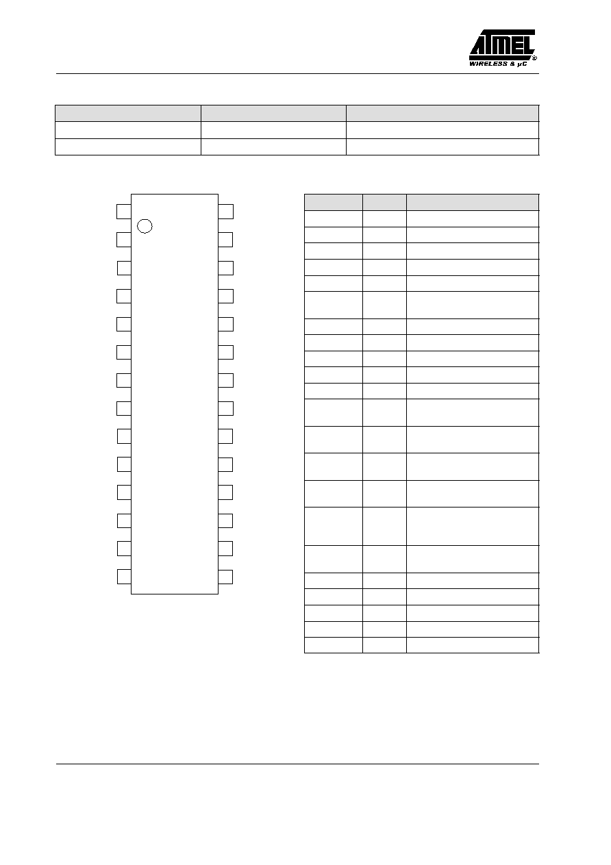
Pin Description
GND
GND
VCC2
CI
TI
CD
PD
PLCK
1
2
3
4
5
6
7
8
10
9
27
22
21
20
18
19
17
12
11
28
25
26
23
24
GND
GND
GND
VCC3
IF
AGC
NRF
GND
TH
RF
SI1
VCC4
16
15
14
13
OSCE
OSCB
PSM
SI2
VCC1
VREF
TANK
GND
Figure 2. Pinning
Pin
Symbol
Function
1
PSM
Power save mode
2
SI2
Control input
3
VCC1
Supply voltage VCO
4
VREF
Reference pin of VCO
5
TANK
Tank pin of VCO
6, 7, 8, 21,
22, 23, 24
GND
Ground
9
VCC2
Supply voltage PLL
10
CI
Control input
11
TI
Test interface
12
CD
Active filter output
13
PD
Tristate charge pump output
14
PLCK
Lock-indication output
(open collector)
15
OSCB
Input of internal oscillator/
buffer
16
OSCE
Output of internal oscillator/
buffer
17
TH
Threshold voltage of compa-
rator
18
AGC
Charge-pump output of
comparator, AGC input for
amplifier and mixer
19
IF
Intermediate frequency out-
put
20
VCC3
Supply voltage
25
NRF
RF input (inverted)
26
RF
RF input
27
SI1
Control input
28
VCC4
Supply voltage
Functional Description
The U2730B-N is an L-band down-converter circuit
covering a gain controlled amplifier, a gain controlled
mixer, an output buffer, a gain control circuitry, an L-band
oscillator and a frequency synthesizer block. Designed
for applications in an DAB receiver the purpose of this
circuit is to down-convert incoming L-band signals in the
frequency range between 1452 MHz and 1492 MHz to an
IF frequency in the range between about 190 MHz and
230 MHz which can be handled by a subsequent DAB
tuner. A block diagram of this circuit is shown in figure 1.

U2730B-N
Preliminary Information
Rev. A2, 06-Oct-00
3 (14)
A main difference to the U2730B is an enhanced IM3 re-
jection. By varying the value of resistor R
TH
a power
threshold between about ≠33 dBm and ≠20 dBm at IF≠
port can be selected.
Gain-Controlled Amplifier
RF signals applied to the input Pin `RF' are amplified by
a gain-controlled amplifier. The complementary
Pin NRF is not internally blocked, it is recommended to
block this pin carefully by an external capacitor. The
gain-control voltage is generated by an internal gain-con-
trol circuitry. The output signal of this amplifier is fed to
a gain-controlled mixer.
Gain-Controlled Mixer and Output Buffer
The purpose of this mixer is to down-convert the L-band
signal in the frequency range of 1452 MHz to 1492 MHz
to an IF frequency in the range of about 190 MHz to
230 MHz. Like the amplifier, the gain of the mixer is
controlled by the gain-control circuitry. The IF signal is
buffered and filtered by a one-pole lowpass filter at a
3-dB frequency of about 500 MHz and then it is fed to the
single-ended output Pin IF.
Gain-Control Circuitry
The purpose of the gain-control circuitry is to measure the
signal power, to compare it with a certain power level and
to generate control voltages for the gain-controlled
amplifier and mixer. An equivalent circuit of this
functional block is shown in figure 6.
In order to meet this functionality, the output signal of the
buffer amplifier is weakly bandpass filtered (transition
range about 60 MHz to 550 MHz), rectified, lowpass
filtered and fed to a comparator whose threshold can be
defined by an external resistor, R
TH
, at Pin TH. By
varying the value of this resistor, a power threshold of
about ≠33 dBm to ≠20 dBm can be selected. In order to
achieve a good intermodulation ratio, it is recommended
to keep the power threshold below ≠25 dBm. An
appropriate application is shown in figure 3. Depending
on the selection made by the comparator, a charge pump
charges or discharges a capacitor which is applied to the
Pin
AGC. By varying this capacitor, different time
constants of the AGC loop can be realized. The voltage
arising at the Pin AGC is used to control the gain setting
of the gain-controlled amplifier and mixer. The voltage at
Pin AGC is in the range of 5.75 V for maximum gain and
0.3 V for minimum gain. This voltage can be use to con-
trol a dual-gate GaAs-FET in front of the U2730B-N to
archieve an extended AGC≠range. By applying an exter-
nal voltage to the Pin AGC, the internal AGC loop can be
overdriven.
Voltage-Controlled Oscillator
A voltage-controlled oscillator supplies an LO signal to
the mixer. An equivalent circuit of this oscillator is shown
in figure 7. In the application circuits figures 7 and 8, a
ceramic coaxial resonator is applied to the oscillator's
Pins TANK and VREF. It should be noted that the
Pin REF has to be blocked carefully. Figure 8 shows a
different application where the oscillator is overdriven by
an external oscillator. In any case, a DC path at a low
impedance must be established between the Pins TANK
and VREF. The output signal of the oscillator is fed to the
LO divider block of the frequency synthesizer unit which
locks the VCO's frequency on the frequency of a refer-
ence oscillator. Figure 12 shows the typical phase-noise
performance of the oscillator in locked state.
Overall Properties of the Signal Path
The overall gain of this circuit amounts 24 dB, the gain-
control range is about 30 dB. With a new AGC-concept
in the amplifier and mixer the U2730B-N reach better in-
termodulation distance (DIM3) at higher IF output power
levels.
Power Save Mode
In different to the U2730B-B the new version offers a
power save function. For V
PSM
> 2 V (Pin 1) the power
consumption in the analog part (gain-controlled amplifier
and mixer and gain-controlled circuitry) is reduced by
80%. The VCO and the PLL is not influenced by the pow-
er-down mode.
Frequency Synthesizer
The frequency synthesizer block consists of reference os-
cillator, a reference divider, an LO divider in order to
divide the frequency of the internal oscillator, a tri≠state
phase detector, a lock detector, a programmable charge
pump, a loop filter amplifier, a control interface and a test
interface. The control interface is accessed by three con-
trol Pins `CI', `SI1' and `SI2'. The test interface provides
test signals which represent output signals of the refer-
ence and the LO divider.
The purpose of this unit is to lock the frequency f
VCO
of
the internal VCO on the frequency f
ref
of the reference
signal applied to the input Pin OSCB a phase-locked loop
according to the following relation:
f
VCO
= SF
f
ref
/ SF
ref
where:
SF = 2464,
SF
ref
scaling factor of reference divider
according to table 1
U2730B-N
Rev. A2, 06-Oct-00
Preliminary Information
4 (14)
Table 1 Scaling factors of the reference frequency
Voltage at Pin SI1
Voltage at Pin SI2
SF
ref
Reference Oscillator Frequency
GND
OPEN
36
18.432 MHz
GND
VCC
33
GND
GND
48
24.576 MHz
OPEN
OPEN
65
OPEN
VCC
63
OPEN
GND
64
32.768 MHz
VCC
OPEN
35
17.920 MHZ
VCC
VCC
32
16.384 MHz
VCC
GND
49
Reference Oscillator
An on-chip crystal oscillator generates the reference sig-
nal which is fed to the reference divider. By connecting
a quartz crystal to the Pins OSCE, OSCB according to fig-
ure 10, this oscillator generates a highly stable reference
signal. The U2731B (Atmel Wireless & Microcontrollers
one-chip front-end IC) offers the reference signal at Pin
FREF. This reference signal (LC-filtered to suppress the
harmonics) can be used to overdrive the oscillator. In this
application (see figure 11) the reference signal has to be
applied to the Pins OSCB and the Pin OSCE must be left
open.
Reference Divider
Nine different scaling factors of the reference divider can
be selected by different voltage settings at the input Pins
SI1, SI2: 32, 33*, 35, 48, 49*, 65*, 64, 63*. The reference
divider factors resulting in reference oscillator frequen-
cies shown in table 1.
*) These scaling factors result in an output frequency of
the reference divider of 512 kHz. If harmonics of the Bd.
3 VCO are falling in the L-band reception band, this spu-
rious can influence the AGC of U2730B-N. That could be
a problem for small incomming signals. In this case it is
possible to switch the reference divider from n
ref
to
n
ref
+1.
LO Divider
The LO divider is operated at the fixed division ratio
2464. Assuming the settings described in the section
`Reference divider', the oscillator's frequency is
controlled to be 1261.568 MHz in locked state and the
output frequency of the RF divider is 512 kHz.
Phase Comparator,
Charge Pump and Loop Filter
The tristate phase detector causes the charge pump to
source or to sink current at the output Pin PD depending
on the phase relation of its input signals which are
provided by the reference and the RF divider respectively.
By means of the control Pin CI, two different values of
this current can be selected, and furthermore the charge-
pump current can be switched off.
The input of the high-gain amplifier (output Pin CD)
which is implemented in order to construct a loop filter,
as shown in the application circuit, can be switched to
GND by means of the control Pin CI (see table 2). In the
application circuit figure 3, the loop filter is completed by
connecting the Pins PD and CD by an appropriate RC
network.
Lock Detector
An internal lock detector checks if the phase difference of
the input signals of the phase detector is smaller than
approximately 250 ns in seven subsequent comparisons.
If a phase lock is detected, the open collector output
Pin PLCK is set to HIGH. It should be noted that the
output current of this pin must be limited by external
circuitry as it is not limited internally. If the voltage at the
control Pin CI is chosen to be half the supply voltage, or
if this control pin is left open, the lock-detector function
is de-activated and the logical value of the PLCK output
is undefined.
Testinterface
If the input control Pin CI is left open (high impedance
state), a test signal which monitors the output frequency
of the reference divider appears at the output Pin TI.
In analogy to the reference divider a test signal which
monitors the output frequency of the RF divider appears
at the test interface output Pin TI if the input control Pin
CI is connect to VCC/2.
U2730B-N
Preliminary Information
Rev. A2, 06-Oct-00
5 (14)
Table 2
Control -interface (CI) settings
CI
PD
PLCK
TI
GND
200
µ
A
ok
≠
Vs
300
µ
A
ok
≠
VCC/2
0
µ
A
Undefined
RF divider
Open
Connected to GND
Undefined
Reference divider
Absolute Maximum Ratings
Parameters
Symbol
Value
Unit
Supply voltage
Pins 3, 9, 20 and 28
V
CC
≠0.3 to +9.5
V
RF input voltage
Pins 25 and 26
V
RF
750
mV
pp
Voltage at Pin AGC
Pin 18
V
AGC
0.5 to 6
V
Voltage at Pin TH
Pin 17
V
TH
≠0.3 to +4.0
V
Input voltage at Pin TANK
(internal oscillator overdriven)
Pin 5
V
TANK
1
V
pp
Current at IF output
Pin 19
I
IF
4.0
mA
Reference input voltage (diff.)
Pin 15
OSCB
1
V
pp
Control input voltage
Pins 1, 2, 10 and 27
CI, SI1,
SI2, PD
≠0.3 to +9.5
V
PLCK output current
Pin 14
I
PLCK
0.5
mA
PLCK output voltage
Pin 14
V
PLCK
≠0.3 to +5.5
V
Junction temperature
T
j
125
∞
C
Storage temperature
T
stg
≠40 to +125
∞
C
Operating Range
Parameter
Symbol
Value
Unit
Supply voltage
Pins 3, 9, 20 and 28
V
CC
8.00 to 9.35
V
Ambient temperature
T
amb
≠40 to +85
∞
C
Thermal Resistance
Parameter
Symbol
Value
Unit
Junction ambient
SSO28 (mod.)
R
thJA
t.b.d.
K/W