Rev. 4734A≠RKE≠11/03
Features
∑
Very High Transmitting Frequency Accuracy Compared to SAW Solutions
(Enables Receivers at Lower Bandwidth than with SAW Resonators)
∑
Lower Cost than the Usual Discrete Solutions Using SAW and Transistors
∑
Supply Voltage 2.2 V to 4.0 V in the Temperature Range of -40
∞
C to 85
∞
C
∑
XTO Output for Clocking the Microcontroller, Thereby Together with the ATAR090 or
ATAR890 Results in the Optimum System Cost-effectiveness
∑
One-chip Solution with Minimum External Circuitry
∑
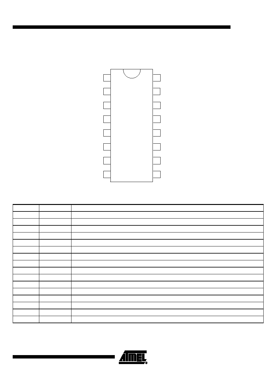
Very Small SSO16 Package, Pitch 0.635, 150 mil
∑
"Single-ended Open-collector" Output (Same Antennas Can Be Used as in Discrete
Solutions, Simpler Adaptation of Magnetic Loop Antennas)
∑
ESD Protection According to MIL-STD.883 (4 KV HBM) Except Pins XTO1/ 2,
ANT and LF
Electrostatic sensitive device.
Observe precautions for handling.
Description
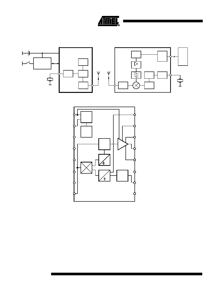
The U2745B is a PLL transmitter IC which has been especially developed for the
demands of RF low-cost data transmission systems at data rates up to 20 kBaud.
The transmitting frequency range is 310 MHz to 440 MHz. It can be used in ASK sys-
tems. The main applications of the U2745B are in the areas of outside temperature
metering, socket control, garage door opener, consumption metering, light/fan or air-
condition control, jalousies, wireless keyboard and various other consumer market
applications.
UHF ASK
Transmitter
U2745B

4
U2745B
4734A≠RKE≠11/03
General Description
The fully integrated VCO and the "single-ended open-collector" output allow particularly
simple, low-cost RF miniature transmitters to be assembled. The single-ended output
enables a considerably simplified adaptation of both a magnetic loop antenna of any
form or a
l
/4 antenna. This is because the load impedance must not be balanced as
would be the case with a differential output.
The XTO's frequency can be selected to be either 13.56 MHz or 9.844 MHz (USA). At
these frequencies, crystals have a very fast start-up time (< 1.5 ms), whereby a wait
time of 5 to 10 ms is required until the transmitter IC is locked. This means that the pro-
cessor does not need to poll a lock detect output.
Functional
Description
ASK Transmission
The U2745B is activated by EN = V
S
. V
ASK
must remain 0 V for 5 ms, then the output
power can be modulated by means of pin ASK. V
EN
remains = V
S
during the transmis-
sion of the message. The ASK input activates the power amplifier and the PLL.
Take-over of the Clock
Pulse in the
Microcontroller
The clock of the crystal oscillator can be used for clocking the microcontroller. The
ATAR090 and ATAR890 have the special feature of starting with an integrated RC oscil-
lator to switch on the U2745B with V
EN
= V
S
. 5 ms later, the 3.39-MHz clock frequency is
present, so that the message can be sent with crystal accuracy.
Application Circuit
The following component values are recommendations for a typical application. C
4
, C
5
,
and C
6
are block capacitors. The values of these capacitors depend on the board layout.
C
4
= 1 nF, C
5
= 1 nF, and C
6
= 22 nF are typically used here. For C
5
, the impedance
between f = 100 MHz and f = 1 GHz should be as low as possible.
C
Loop1
and C
Loop2
are selected so that the antenna oscillates in resonance and the adap-
tation to the appropriate impedance transformation is possible.
L
F e e d
is an inductor for the antenna's DC current supply. A typical value is
L
Feed
= 220 nH. L
Feed
can be either printed on the PC board or be a discrete component.
Output Power
Measurement
The following output network (see Figure 4 on page 5) can be used for output power
evaluation, the exact values of L
10
and C
10
are dependent on the layout.
L
10
and C
10
form the transformation network to adopt the output impedance of the IC to
50
W
. The following table shows the values for an output power of 2 mW and an
R
PWRSET
= 1.2 k
W
.
Table 1.
Transformation Network
f/MHz
C10/pF
L10/nH
Z
Load_opt
/
W
315
2.7
56
260 + j330
433.92
1.8
33
185 + j268