 | –≠–ª–µ–∫—Ç—Ä–æ–Ω–Ω—ã–π –∫–æ–º–ø–æ–Ω–µ–Ω—Ç: U2760B | –°–∫–∞—á–∞—Ç—å:  PDF PDF  ZIP ZIP |

U2760B
Rev. A5, 07-Sep-00
1 (14)
CT2 RX/TX IC
Description
The IC U2760B for digital cordless telephone applica-
tions is fabricated using Atmel Wireless &
Microcontrollers' most advanced UHF process. It covers
the CT2 band (864 MHz to 868 MHz) as well as the CT2
Plus band (up to 952 MHz). The RX/TX circuit provides
the down-conversion to the data stream and the up
conversion from the first IF. Along with Atmel Wireless
& Microcontrollers' RF front end, Twin PLL, I/Q
modulator and AMDs CT2 PhoX
TM
controller
AM 79C4xx, a complete CT2 IC kit is available.
Electrostatic sensitive device.
Observe precautions for handling.
Features
D Low supply voltage 2.9 V typical (min. 2.7 V)
D Provides down-conversion to the data stream,
up-conversion from the first IF
D Integrated UHF and VHF VCOs
D Low noise figure of RX path (NF v 10 dB)
D RX and TX power down
D First IF filter used for transmit as well receive mode
D Temperature-compensated logarithmic Receiver
Signal Strength Indicator (RSSI) with a dynamic
range of 75 dB
D Low power consumption in RX and TX mode
(<20 mA typ.)
D SSO28 plastic package
Benefits
D Low power consumption results in extended talk time
D Few external components and very small package
save space
Block Diagram (Simplified Schematic)
MX1
MX2
MX4
MX3
VCO1
VCO2
LIMIT
RSSI
RSSI out
DEMOD
RXdata
RX enable
MX1 in
MX4 outn
MX1/3
outp
VCO1 ref
VCO1 tank
VCO1 out
VCO2
ref
VCO2
tank
VCO2
out
MX3 in
DEMOD out
COMP cap
COMP in
MX1/3
outn
MX2/4
nin
MX2 out
LIMIT in
QUAD
TX enable
VCC
vco/lf
VCC
GND
vco/lf
GND
MX4 outp
26
25
2
28
4
20
19
27
11
12
13
10
18
16
17
3
8
9
24
23
22
5
6
7
21
15
14
COMP
10 pF
100k
W
100k
W
94 9532
1
MX2/4
in
Figure 1. Block diagram (simplified schematic)

U2760B
Rev. A5, 07-Sep-00
2 (14)
Ordering Information
Extended Type Number
Package
Remarks
U2760B-AFS
SSO28
Tube, MOQ 600 pcs.
U2760B-AFSG3
SSO28
Taped and reeled, MOQ 4000 pcs.
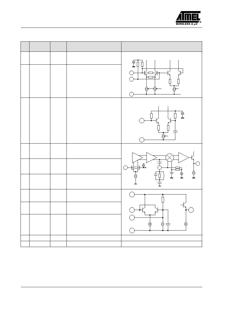
Functional Description
MX1
Mixer 1 converts the RF signal to the first IF. It has a high
impedance, asymmetrical input and a symmetrical open
collector output.
MX2
The second mixer provides the down conversion to the
second IF. An external SAW filter is conected to the input
to provide rejection of the image frequency and spurious
signals that went through the RF filtering.
LIMITER / RSSI
This block contains a high-gain (100 dB) amplifier,
providing a limited signal at the second IF frequency for
the demodulation, as well as a signal-strength indicator
providing an output voltage proportional to the input
power.
DEMOD
The quadrature demodulator in the receiving path
contains an internal 10-pF quadrature capacitor to couple
the IF signal to the external tank providing the 90 degree
phase shift. An external bit slicer reshapes the bits, a
sample and hold circuit maintains the average DC value
at the demodulator when switching the signal between
transmission and reception.
COMP
The comparator circuit with 100-k
W input resistor and
external input biasing has a 10-mV hysteresis. It is
designed to square up the demodulated data signal.
MX3
The third mixer converts the 800-kHz signal coming from
the modulator circuit to the IF frequency. It has a high
impedance, asymmetrical input and a symmetrical open
collector output.
MX4
This mixer is designed for the up conversion of the RF
frequency. It has a high impedance, unsymmetrical input
and a symmetrical open collector output. The image
rejection is obtained by external RF filtering.
The same first IF filter is used for the transmit as well as
the receive path. In the transmit path, this filter is
supposed to eliminate the mixing products from MX3, in
particular, the harmonics of the IF frequency.
VCO1
The UHF VCO covers the frequency band up to
700 MHz. For external VCO applications this circuit can
be used as a buffer stage.
VCO2
This VCO covers a frequency band up to 400 MHz.

U2760B
Rev. A5, 07-Sep-00
3 (14)
Pin Description
Pin
Symbol
Function
¡¡¡
¡¡¡
¡¡¡
1
¡¡¡¡¡
¡¡¡¡¡
¡¡¡¡¡
MX2/4in
¡¡¡¡¡¡¡¡¡¡
¡¡¡¡¡¡¡¡¡¡
¡¡¡¡¡¡¡¡¡¡
Mixer 2/ Mixer 4 input
2
MX2/4nin
Mixer 2/ Mixer 4 ref. input
¡¡¡
¡¡¡
3
¡¡¡¡¡
¡¡¡¡¡
MX3in
¡¡¡¡¡¡¡¡¡¡
¡¡¡¡¡¡¡¡¡¡
Mixer 3 input
¡¡¡
¡¡¡
4
¡¡¡¡¡
¡¡¡¡¡
LIMITin
¡¡¡¡¡¡¡¡¡¡
¡¡¡¡¡¡¡¡¡¡
Limiter/RSSI input
¡¡¡
¡¡¡
5
¡¡¡¡¡
¡¡¡¡¡
VCO1out
¡¡¡¡¡¡¡¡¡¡
¡¡¡¡¡¡¡¡¡¡
VCO1 output (to PLL)
¡¡¡
¡¡¡
6
¡¡¡¡¡
¡¡¡¡¡
VCO1tank
¡¡¡¡¡¡¡¡¡¡
¡¡¡¡¡¡¡¡¡¡
VCO1 resonator
¡¡¡
¡¡¡
¡¡¡
7
¡¡¡¡¡
¡¡¡¡¡
¡¡¡¡¡
VCO1ref
¡¡¡¡¡¡¡¡¡¡
¡¡¡¡¡¡¡¡¡¡
¡¡¡¡¡¡¡¡¡¡
VCO1 resonator, to be blocked
¡¡¡
¡¡¡
8
¡¡¡¡¡
¡¡¡¡¡
GNDvco/lf
¡¡¡¡¡¡¡¡¡¡
¡¡¡¡¡¡¡¡¡¡
Ground VCO, low frequency
parts
¡¡¡
¡¡¡
¡¡¡
9
¡¡¡¡¡
¡¡¡¡¡
¡¡¡¡¡
VCCvco/lf
¡¡¡¡¡¡¡¡¡¡
¡¡¡¡¡¡¡¡¡¡
¡¡¡¡¡¡¡¡¡¡
Power supply VCO/LF parts
¡¡¡
¡¡¡
10
¡¡¡¡¡
¡¡¡¡¡
RXdata
¡¡¡¡¡¡¡¡¡¡
¡¡¡¡¡¡¡¡¡¡
RX data output
¡¡¡
¡¡¡
11
¡¡¡¡¡
¡¡¡¡¡
QUAD
¡¡¡¡¡¡¡¡¡¡
¡¡¡¡¡¡¡¡¡¡
Quadrature filter
¡¡¡
¡¡¡
¡¡¡
12
¡¡¡¡¡
¡¡¡¡¡
¡¡¡¡¡
DEMOD-
out
¡¡¡¡¡¡¡¡¡¡
¡¡¡¡¡¡¡¡¡¡
¡¡¡¡¡¡¡¡¡¡
Demodulator output
¡¡¡
¡¡¡
13
¡¡¡¡¡
¡¡¡¡¡
COMPin
¡¡¡¡¡¡¡¡¡¡
¡¡¡¡¡¡¡¡¡¡
Comparator input
¡¡¡
¡¡¡
14
¡¡¡¡¡
¡¡¡¡¡
COMPcap
¡¡¡¡¡¡¡¡¡¡
¡¡¡¡¡¡¡¡¡¡
Comparator blocking capacitor
¡¡¡
¡¡¡
15
¡¡¡¡¡
¡¡¡¡¡
RXenable
¡¡¡¡¡¡¡¡¡¡
¡¡¡¡¡¡¡¡¡¡
RX enable
¡¡¡
¡¡¡
16
¡¡¡¡¡
¡¡¡¡¡
VCO2out
¡¡¡¡¡¡¡¡¡¡
¡¡¡¡¡¡¡¡¡¡
VCO2 output (to PLL)
¡¡¡
¡¡¡
17
¡¡¡¡¡
¡¡¡¡¡
VCO2ref
¡¡¡¡¡¡¡¡¡¡
¡¡¡¡¡¡¡¡¡¡
VCO2 resonator, to be blocked
¡¡¡
¡¡¡
¡¡¡
18
¡¡¡¡¡
¡¡¡¡¡
¡¡¡¡¡
VCO2tank
¡¡¡¡¡¡¡¡¡¡
¡¡¡¡¡¡¡¡¡¡
¡¡¡¡¡¡¡¡¡¡
VCO2 resonator
¡¡¡
¡¡¡
19
¡¡¡¡¡
¡¡¡¡¡
GND
¡¡¡¡¡¡¡¡¡¡
¡¡¡¡¡¡¡¡¡¡
Ground
¡¡¡
¡¡¡
20
¡¡¡¡¡
¡¡¡¡¡
VCC
¡¡¡¡¡¡¡¡¡¡
¡¡¡¡¡¡¡¡¡¡
Power-supply voltage
¡¡¡
¡¡¡
21
¡¡¡¡¡
¡¡¡¡¡
MX1in
¡¡¡¡¡¡¡¡¡¡
¡¡¡¡¡¡¡¡¡¡
Mixer 1 input
¡¡¡
¡¡¡
22
¡¡¡¡¡
¡¡¡¡¡
MX4outn
¡¡¡¡¡¡¡¡¡¡
¡¡¡¡¡¡¡¡¡¡
Mixer 4 output n
¡¡¡
¡¡¡
23
¡¡¡¡¡
¡¡¡¡¡
MX4outp
¡¡¡¡¡¡¡¡¡¡
¡¡¡¡¡¡¡¡¡¡
Mixer 4 output p
¡¡¡
¡¡¡
¡¡¡
24
¡¡¡¡¡
¡¡¡¡¡
¡¡¡¡¡
TXenable
¡¡¡¡¡¡¡¡¡¡
¡¡¡¡¡¡¡¡¡¡
¡¡¡¡¡¡¡¡¡¡
TX enable
¡¡¡
¡¡¡
25
¡¡¡¡¡
¡¡¡¡¡
MX1/3outn
¡¡¡¡¡¡¡¡¡¡
¡¡¡¡¡¡¡¡¡¡
Mixer 1/ Mixer 3 output n
¡¡¡
¡¡¡
26
¡¡¡¡¡
¡¡¡¡¡
MX1/3outp
¡¡¡¡¡¡¡¡¡¡
¡¡¡¡¡¡¡¡¡¡
Mixer 1/ Mixer 3 output p
¡¡¡
¡¡¡
27
¡¡¡¡¡
¡¡¡¡¡
RSSIout
¡¡¡¡¡¡¡¡¡¡
¡¡¡¡¡¡¡¡¡¡
Signal-strength output
¡¡¡
¡¡¡
28
¡¡¡¡¡
¡¡¡¡¡
MX2out
¡¡¡¡¡¡¡¡¡¡
¡¡¡¡¡¡¡¡¡¡
Mixer 2 output
1
2
3
4
5
6
7
8
10
9
27
22
21
20
18
19
17
12
11
28
25
26
23
24
VCO1tank
VCO1ref
GNDvco/If
VCCvco/If
RXdata
QUAD
LIMITin
VCO1out
DEMODout
MX3in
MX2/4nin
MX2/4in
MX4outp
MX4outn
MX1in
VCC
GND
VCO2tank
MX1/3outn
TXenable
VCO2ref
MX1/3outp
RSSIout
MX2out
16
15
14
13
COMPin
COMPcab
VCO2out
RXenable
Figure 2. Pinning
U2760B
Rev. A5, 07-Sep-00
4 (14)
Pin Functions
Pin
Symbol
Pin
Voltage
Function
Equivalent Circuit
¡¡
¡¡
¡¡
1
¡¡¡¡¡
¡¡¡¡¡
¡¡¡¡¡
MX2/4in
¡¡¡¡
¡¡¡¡
¡¡¡¡
1.5
¡¡¡¡¡¡¡¡¡¡
¡¡¡¡¡¡¡¡¡¡
¡¡¡¡¡¡¡¡¡¡
Mixer 2/ Mixer 4 input
¡¡¡¡¡¡¡¡¡¡¡¡¡¡¡
¡¡¡¡¡¡¡¡¡¡¡¡¡¡¡
¡¡¡¡¡¡¡¡¡¡¡¡¡¡¡
To MX4
To MX2
2
MX2/4nin
1.5
Mixer 2/ Mixer 4 complementary
input
Pin 1 is the input of the mixers, Pin 2
can either be used for differential
input signals, or should be connected
to GND via a bypass capacitor
¡¡¡¡¡¡¡¡¡¡¡¡¡¡¡
¡¡¡¡¡¡¡¡¡¡¡¡¡¡¡
¡¡¡¡¡¡¡¡¡¡¡¡¡¡¡
¡¡¡¡¡¡¡¡¡¡¡¡¡¡¡
¡¡¡¡¡¡¡¡¡¡¡¡¡¡¡
¡¡¡¡¡¡¡¡¡¡¡¡¡¡¡
¡¡¡¡¡¡¡¡¡¡¡¡¡¡¡
RX
TX
1
2
19
¡¡
¡¡
¡¡
¡¡
¡¡
¡¡
¡¡
¡¡
¡¡
3
¡¡¡¡¡
¡¡¡¡¡
¡¡¡¡¡
¡¡¡¡¡
¡¡¡¡¡
¡¡¡¡¡
¡¡¡¡¡
¡¡¡¡¡
¡¡¡¡¡
MX3in
¡¡¡¡
¡¡¡¡
¡¡¡¡
¡¡¡¡
¡¡¡¡
¡¡¡¡
¡¡¡¡
¡¡¡¡
¡¡¡¡
1.7 (RX)
2.4 (TX)
¡¡¡¡¡¡¡¡¡¡
¡¡¡¡¡¡¡¡¡¡
¡¡¡¡¡¡¡¡¡¡
¡¡¡¡¡¡¡¡¡¡
¡¡¡¡¡¡¡¡¡¡
¡¡¡¡¡¡¡¡¡¡
¡¡¡¡¡¡¡¡¡¡
¡¡¡¡¡¡¡¡¡¡
¡¡¡¡¡¡¡¡¡¡
Mixer 3 input
complementary input is internally
connected to GND via a bypass
capacitor
¡¡¡¡¡¡¡¡¡¡¡¡¡¡¡
¡¡¡¡¡¡¡¡¡¡¡¡¡¡¡
¡¡¡¡¡¡¡¡¡¡¡¡¡¡¡
¡¡¡¡¡¡¡¡¡¡¡¡¡¡¡
¡¡¡¡¡¡¡¡¡¡¡¡¡¡¡
¡¡¡¡¡¡¡¡¡¡¡¡¡¡¡
¡¡¡¡¡¡¡¡¡¡¡¡¡¡¡
¡¡¡¡¡¡¡¡¡¡¡¡¡¡¡
¡¡¡¡¡¡¡¡¡¡¡¡¡¡¡
To MX3
TX
3
19
¡¡
¡¡
¡¡
4
¡¡¡¡¡
¡¡¡¡¡
¡¡¡¡¡
LIMITin
¡¡¡¡
¡¡¡¡
¡¡¡¡
2.1
¡¡¡¡¡¡¡¡¡¡
¡¡¡¡¡¡¡¡¡¡
¡¡¡¡¡¡¡¡¡¡
Limiter/RSSI input
¡¡¡¡¡¡¡¡¡¡¡¡¡¡¡
¡¡¡¡¡¡¡¡¡¡¡¡¡¡¡
¡¡¡¡¡¡¡¡¡¡¡¡¡¡¡
Vcc
¡¡
¡¡
¡¡
¡¡
11
¡¡¡¡¡
¡¡¡¡¡
¡¡¡¡¡
¡¡¡¡¡
QUAD
¡¡¡¡
¡¡¡¡
¡¡¡¡
¡¡¡¡
1.5
¡¡¡¡¡¡¡¡¡¡
¡¡¡¡¡¡¡¡¡¡
¡¡¡¡¡¡¡¡¡¡
¡¡¡¡¡¡¡¡¡¡
Quadrature filter
¡¡¡¡¡¡¡¡¡¡¡¡¡¡¡
¡¡¡¡¡¡¡¡¡¡¡¡¡¡¡
¡¡¡¡¡¡¡¡¡¡¡¡¡¡¡
¡¡¡¡¡¡¡¡¡¡¡¡¡¡¡
Vcc
Ref
10pF
4
11
12
¡¡
¡¡
¡¡
12
¡¡¡¡¡
¡¡¡¡¡
¡¡¡¡¡
DEMODout
¡¡¡¡
¡¡¡¡
¡¡¡¡
1.2
¡¡¡¡¡¡¡¡¡¡
¡¡¡¡¡¡¡¡¡¡
¡¡¡¡¡¡¡¡¡¡
Demodulator output
¡¡¡¡¡¡¡¡¡¡¡¡¡¡¡
¡¡¡¡¡¡¡¡¡¡¡¡¡¡¡
¡¡¡¡¡¡¡¡¡¡¡¡¡¡¡
¡¡
¡¡
¡¡
5
¡¡¡¡¡
¡¡¡¡¡
¡¡¡¡¡
VCO1out
¡¡¡¡
¡¡¡¡
¡¡¡¡
1.1
¡¡¡¡¡¡¡¡¡¡
¡¡¡¡¡¡¡¡¡¡
¡¡¡¡¡¡¡¡¡¡
VCO1 output (to PLL)
¡¡¡¡¡¡¡¡¡¡¡¡¡¡¡
¡¡¡¡¡¡¡¡¡¡¡¡¡¡¡
¡¡¡¡¡¡¡¡¡¡¡¡¡¡¡
9
¡¡
¡¡
¡¡
¡¡
6
¡¡¡¡¡
¡¡¡¡¡
¡¡¡¡¡
¡¡¡¡¡
VCO1tank
¡¡¡¡
¡¡¡¡
¡¡¡¡
¡¡¡¡
1.5
¡¡¡¡¡¡¡¡¡¡
¡¡¡¡¡¡¡¡¡¡
¡¡¡¡¡¡¡¡¡¡
¡¡¡¡¡¡¡¡¡¡
VCO1 resonator
¡¡¡¡¡¡¡¡¡¡¡¡¡¡¡
¡¡¡¡¡¡¡¡¡¡¡¡¡¡¡
¡¡¡¡¡¡¡¡¡¡¡¡¡¡¡
¡¡¡¡¡¡¡¡¡¡¡¡¡¡¡
6
5
¡¡
¡¡
¡¡
¡¡
7
¡¡¡¡¡
¡¡¡¡¡
¡¡¡¡¡
¡¡¡¡¡
VCO1ref
¡¡¡¡
¡¡¡¡
¡¡¡¡
¡¡¡¡
1.5
¡¡¡¡¡¡¡¡¡¡
¡¡¡¡¡¡¡¡¡¡
¡¡¡¡¡¡¡¡¡¡
¡¡¡¡¡¡¡¡¡¡
VCO1 reference, to be blocked. This
Pin is also internally connected to
GND via a bypass capacitor
¡¡¡¡¡¡¡¡¡¡¡¡¡¡¡
¡¡¡¡¡¡¡¡¡¡¡¡¡¡¡
¡¡¡¡¡¡¡¡¡¡¡¡¡¡¡
¡¡¡¡¡¡¡¡¡¡¡¡¡¡¡
7
8
¡¡
¡¡
8
¡¡¡¡¡
¡¡¡¡¡
GNDvco/lf
¡¡¡¡
¡¡¡¡
≠
¡¡¡¡¡¡¡¡¡¡
¡¡¡¡¡¡¡¡¡¡
Ground VCO, low frequency parts
¡¡¡¡¡¡¡¡¡¡¡¡¡¡¡
¡¡¡¡¡¡¡¡¡¡¡¡¡¡¡
¡¡
¡¡
9
¡¡¡¡¡
¡¡¡¡¡
VCCvco/lf
¡¡¡¡
¡¡¡¡
≠
¡¡¡¡¡¡¡¡¡¡
¡¡¡¡¡¡¡¡¡¡
Power supply VCO/LF parts
¡¡¡¡¡¡¡¡¡¡¡¡¡¡¡
¡¡¡¡¡¡¡¡¡¡¡¡¡¡¡

U2760B
Rev. A5, 07-Sep-00
5 (14)
Equivalent Circuit
Function
Pin
Voltage
Symbol
Pin
¡¡¡
¡¡¡
¡¡¡
10
¡¡¡¡
¡¡¡¡
¡¡¡¡
RXdata
¡¡¡¡
¡¡¡¡
¡¡¡¡
0 to 2.9
¡¡¡¡¡¡¡¡¡¡
¡¡¡¡¡¡¡¡¡¡
¡¡¡¡¡¡¡¡¡¡
RX data output
¡¡¡¡¡¡¡¡¡¡¡¡¡¡¡
¡¡¡¡¡¡¡¡¡¡¡¡¡¡¡
¡¡¡¡¡¡¡¡¡¡¡¡¡¡¡
Vcc
50k
¡¡¡
¡¡¡
¡¡¡
¡¡¡
13
¡¡¡¡
¡¡¡¡
¡¡¡¡
¡¡¡¡
COMPin
¡¡¡¡
¡¡¡¡
¡¡¡¡
¡¡¡¡
1.2
¡¡¡¡¡¡¡¡¡¡
¡¡¡¡¡¡¡¡¡¡
¡¡¡¡¡¡¡¡¡¡
¡¡¡¡¡¡¡¡¡¡
Comparator input
¡¡¡¡¡¡¡¡¡¡¡¡¡¡¡
¡¡¡¡¡¡¡¡¡¡¡¡¡¡¡
¡¡¡¡¡¡¡¡¡¡¡¡¡¡¡
¡¡¡¡¡¡¡¡¡¡¡¡¡¡¡
100k
50k
10
13
¡¡¡
¡¡¡
¡¡¡
14
¡¡¡¡
¡¡¡¡
¡¡¡¡
COMPcap
¡¡¡¡
¡¡¡¡
¡¡¡¡
1.2
¡¡¡¡¡¡¡¡¡¡
¡¡¡¡¡¡¡¡¡¡
¡¡¡¡¡¡¡¡¡¡
Comparator blocking capacitor
¡¡¡¡¡¡¡¡¡¡¡¡¡¡¡
¡¡¡¡¡¡¡¡¡¡¡¡¡¡¡
¡¡¡¡¡¡¡¡¡¡¡¡¡¡¡
100k
14
13
¡¡¡
¡¡¡
¡¡¡
¡¡¡
¡¡¡
¡¡¡
15
¡¡¡¡
¡¡¡¡
¡¡¡¡
¡¡¡¡
¡¡¡¡
¡¡¡¡
RXenable
¡¡¡¡
¡¡¡¡
¡¡¡¡
¡¡¡¡
¡¡¡¡
¡¡¡¡
≠
¡¡¡¡¡¡¡¡¡¡
¡¡¡¡¡¡¡¡¡¡
¡¡¡¡¡¡¡¡¡¡
¡¡¡¡¡¡¡¡¡¡
¡¡¡¡¡¡¡¡¡¡
¡¡¡¡¡¡¡¡¡¡
RX enable
¡¡¡¡¡¡¡¡¡¡¡¡¡¡¡
¡¡¡¡¡¡¡¡¡¡¡¡¡¡¡
¡¡¡¡¡¡¡¡¡¡¡¡¡¡¡
¡¡¡¡¡¡¡¡¡¡¡¡¡¡¡
¡¡¡¡¡¡¡¡¡¡¡¡¡¡¡
¡¡¡¡¡¡¡¡¡¡¡¡¡¡¡
Vcc
15
¡¡¡
¡¡¡
¡¡¡
¡¡¡
16
¡¡¡¡
¡¡¡¡
¡¡¡¡
¡¡¡¡
VCO2out
¡¡¡¡
¡¡¡¡
¡¡¡¡
¡¡¡¡
1.1
¡¡¡¡¡¡¡¡¡¡
¡¡¡¡¡¡¡¡¡¡
¡¡¡¡¡¡¡¡¡¡
¡¡¡¡¡¡¡¡¡¡
VCO2 output (to PLL)
¡¡¡¡¡¡¡¡¡¡¡¡¡¡¡
¡¡¡¡¡¡¡¡¡¡¡¡¡¡¡
¡¡¡¡¡¡¡¡¡¡¡¡¡¡¡
¡¡¡¡¡¡¡¡¡¡¡¡¡¡¡
9
¡¡¡
¡¡¡
¡¡¡
¡¡¡
17
¡¡¡¡
¡¡¡¡
¡¡¡¡
¡¡¡¡
VCO2ref
¡¡¡¡
¡¡¡¡
¡¡¡¡
¡¡¡¡
1.6
¡¡¡¡¡¡¡¡¡¡
¡¡¡¡¡¡¡¡¡¡
¡¡¡¡¡¡¡¡¡¡
¡¡¡¡¡¡¡¡¡¡
VCO2 resonator, to be blocked
¡¡¡¡¡¡¡¡¡¡¡¡¡¡¡
¡¡¡¡¡¡¡¡¡¡¡¡¡¡¡
¡¡¡¡¡¡¡¡¡¡¡¡¡¡¡
¡¡¡¡¡¡¡¡¡¡¡¡¡¡¡
18
16
¡¡¡
¡¡¡
¡¡¡
18
¡¡¡¡
¡¡¡¡
¡¡¡¡
VCO2tank
¡¡¡¡
¡¡¡¡
¡¡¡¡
1.6
¡¡¡¡¡¡¡¡¡¡
¡¡¡¡¡¡¡¡¡¡
¡¡¡¡¡¡¡¡¡¡
VCO2 resonator
¡¡¡¡¡¡¡¡¡¡¡¡¡¡¡
¡¡¡¡¡¡¡¡¡¡¡¡¡¡¡
¡¡¡¡¡¡¡¡¡¡¡¡¡¡¡
17
8
¡¡¡
¡¡¡
19
¡¡¡¡
¡¡¡¡
GND
¡¡¡¡
¡¡¡¡
≠
¡¡¡¡¡¡¡¡¡¡
¡¡¡¡¡¡¡¡¡¡
Ground (mixer parts)
¡¡¡¡¡¡¡¡¡¡¡¡¡¡¡
¡¡¡¡¡¡¡¡¡¡¡¡¡¡¡
¡¡¡
¡¡¡
20
¡¡¡¡
¡¡¡¡
VCC
¡¡¡¡
¡¡¡¡
≠
¡¡¡¡¡¡¡¡¡¡
¡¡¡¡¡¡¡¡¡¡
Power supply (mixer parts)
¡¡¡¡¡¡¡¡¡¡¡¡¡¡¡
¡¡¡¡¡¡¡¡¡¡¡¡¡¡¡
¡¡¡
¡¡¡
¡¡¡
¡¡¡
¡¡¡
¡¡¡
¡¡¡
¡¡¡
¡¡¡
21
¡¡¡¡
¡¡¡¡
¡¡¡¡
¡¡¡¡
¡¡¡¡
¡¡¡¡
¡¡¡¡
¡¡¡¡
¡¡¡¡
MX1in
¡¡¡¡
¡¡¡¡
¡¡¡¡
¡¡¡¡
¡¡¡¡
¡¡¡¡
¡¡¡¡
¡¡¡¡
¡¡¡¡
1.5
¡¡¡¡¡¡¡¡¡¡
¡¡¡¡¡¡¡¡¡¡
¡¡¡¡¡¡¡¡¡¡
¡¡¡¡¡¡¡¡¡¡
¡¡¡¡¡¡¡¡¡¡
¡¡¡¡¡¡¡¡¡¡
¡¡¡¡¡¡¡¡¡¡
¡¡¡¡¡¡¡¡¡¡
¡¡¡¡¡¡¡¡¡¡
Mixer 1 input
complimentary input is internally
connected to GND via a bypass
capacitor
¡¡¡¡¡¡¡¡¡¡¡¡¡¡¡
¡¡¡¡¡¡¡¡¡¡¡¡¡¡¡
¡¡¡¡¡¡¡¡¡¡¡¡¡¡¡
¡¡¡¡¡¡¡¡¡¡¡¡¡¡¡
¡¡¡¡¡¡¡¡¡¡¡¡¡¡¡
¡¡¡¡¡¡¡¡¡¡¡¡¡¡¡
¡¡¡¡¡¡¡¡¡¡¡¡¡¡¡
¡¡¡¡¡¡¡¡¡¡¡¡¡¡¡
¡¡¡¡¡¡¡¡¡¡¡¡¡¡¡
To MX1
RX
21
19
¡¡¡
¡¡¡
¡¡¡
¡¡¡
¡¡¡
22
¡¡¡¡
¡¡¡¡
¡¡¡¡
¡¡¡¡
¡¡¡¡
MX4outn
¡¡¡¡
¡¡¡¡
¡¡¡¡
¡¡¡¡
¡¡¡¡
≠
¡¡¡¡¡¡¡¡¡¡
¡¡¡¡¡¡¡¡¡¡
¡¡¡¡¡¡¡¡¡¡
¡¡¡¡¡¡¡¡¡¡
¡¡¡¡¡¡¡¡¡¡
Mixer 4 output n
¡¡¡¡¡¡¡¡¡¡¡¡¡¡¡
¡¡¡¡¡¡¡¡¡¡¡¡¡¡¡
¡¡¡¡¡¡¡¡¡¡¡¡¡¡¡
¡¡¡¡¡¡¡¡¡¡¡¡¡¡¡
¡¡¡¡¡¡¡¡¡¡¡¡¡¡¡
22
23
¡¡¡
¡¡¡
¡¡¡
¡¡¡
¡¡¡
23
¡¡¡¡
¡¡¡¡
¡¡¡¡
¡¡¡¡
¡¡¡¡
MX4outp
¡¡¡¡
¡¡¡¡
¡¡¡¡
¡¡¡¡
¡¡¡¡
≠
¡¡¡¡¡¡¡¡¡¡
¡¡¡¡¡¡¡¡¡¡
¡¡¡¡¡¡¡¡¡¡
¡¡¡¡¡¡¡¡¡¡
¡¡¡¡¡¡¡¡¡¡
Mixer 4 output p
¡¡¡¡¡¡¡¡¡¡¡¡¡¡¡
¡¡¡¡¡¡¡¡¡¡¡¡¡¡¡
¡¡¡¡¡¡¡¡¡¡¡¡¡¡¡
¡¡¡¡¡¡¡¡¡¡¡¡¡¡¡
¡¡¡¡¡¡¡¡¡¡¡¡¡¡¡
LO1
from
MX4 in