1
Features
∑
Supply-voltage Range: 2.7 V to 5.5 V
∑
Single-ended Output, no Balun Required
∑
Single-ended Input for RF and LO
∑
Excellent Isolation Characteristics
∑
Power-down Mode
∑
IP3 and Compression Point Programmable
∑
2.5-GHz Operating Frequency
Benefits
∑
Reduced System Costs as only Few External Component (no Balun) are Required
∑
Small Package
∑
Very Low Current Consumption
∑
Easy to Use
Electrostatic sensitive device.
Observe precautions for handling.
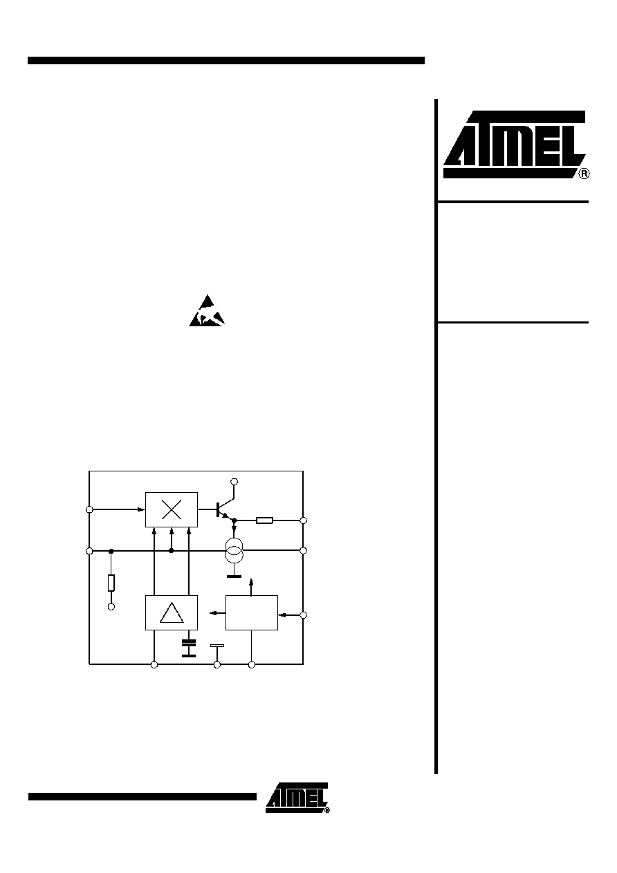
Description
The U2795B is a 2.5-GHz mixer for WLAN and RF telecommunications equipment,
e.g., DECT and PCN. The IC is manufactured using Atmel's advanced bipolar technol-
ogy. A double-balanced approach was chosen to assure good isolation characteristics
and a minimum of spurious products. The input and output are single-ended, and their
characteristics are programmable. No output transformer or balun is required.
Figure 1. Block Diagram
R1
Voltage
regulator
VH
R
V
VS
2
RFi
3
P
VH
7
LO i
6
GND
VS
1
4
8
R2
5 IF
PD
S
o
o
2.5-GHz
Double-
balanced
Mixer
U2795B
Rev. 4654A≠CELL≠01/03

2
U2795B
4654A≠CELL≠01/03
Pin Configuration
Figure 2. Pinning
1
2
3
4
5
6
7
8
V
S
RF
P
IF
O
LO
i
PU
GND
S
O
Pin Description
Pin
Symbol
Function
1
V
S
Supply voltage
2
RF
i
RF input
3
P
Progamming port IP3, CP
4
S
O
Output symmetry
5
IF
O
IF output
6
GND
Ground
7
LO
i
LO input
8
PU
Power-up
3
U2795B
4654A≠CELL≠01/03
Functional Description
Supply Voltage
The IC is designed for a supply-voltage range of 2.7 V to 5.5 V. As the IC is internally
stabilized, the performance of the circuit is nearly independent of the supply voltage.
Input Impedance
The input impedance, Z
RFi
, is about 700
W
with an additional capacitive component. This
condition provides the best noise figure in combination with a matching network.
3rd Order Intercept Point
(IP3)
The voltage divider, R
P
/R
1
, determinates both the input and output intercept point, IIP3
and OIP3. If the value of RP is infinite, the maximum value of IIP3 reachs about -4 dBm.
The IP3/R
P
characteristics are shown in Figure 3 and Figure 4.
Output Impedance and
Intercept Point
The output impedance is shown in Figure 11. Both low output impedance and a high
intercept point are defined to a high value of R
P
.
Current Consumption, I
S
Depending on the chosen input and output conditions of the IC, the current consump-
tion,I
S
, is between 4 mA and 10 mA. The current consumption in dependence of Rp is
shown in Figure 6.
Power-up
This feature provides extended battery lifetime. If this function is not used, Pin 8 has to
be connected to V
S
(Pin 1).
Output Symmetry
The symmetry of the load current can be matched and thus optimized for a given load
impedance.
Absolute Maximum Ratings
Parameters
Symbol
Value
Unit
Supply voltage
V
S
6
V
Input voltage
V
I
0 to V
S
V
Junction temperature
T
j
125
∞
C
Storage-temperature range
T
stg
-40 to +125
∞
C
Thermal Resistance
Parameters
Symbol
Value
Unit
Junction ambient SO8
R
thJA
175
K/W
Operating Range
Parameters
Symbol
Value
Unit
Supply-voltage range
V
S
2.7 to 5.5
V
Ambient-temperature range
T
amb
-40 to +85
∞
C

4
U2795B
4654A≠CELL≠01/03
Electrical Characteristics
V
S
= 3 V, f
LOi
= 1 GHz, IF = 900 MHz, RF = 100 MHz, R
P
=
•
, system impedance Zo = 50
W
, T
amb
= 25
∞
C, R
T
= 56
W
reference point Pin 6, unless otherwise specified
No.
Parameters
Test Conditions
Pin
Symbol
Min.
Typ.
Max.
Unit
Type*
1.1
Supply voltage range
1
V
S
2.7
5.5
V
A
1.2
Supply Current
VS = 2.7 V
1
1
I
S
I
S
9
3
13
6.2
mA
mA
A
A
1.3
Conversion Supply
Current
R
L
= 50
W
, R
T
=
•
R
L
=
50
W
, R
T
= 56
W
1
PG
C
PG
C
9
4
dB
dB
B
2
Operating Frequencies
2.1
RF
i
frequency
2
RF
i
10
2500
MHz
D
2.2
LO
i
frequency
7
f
LOi
50
2500
MHz
D
2.3
IF
o
frequency
5
f
IFo
50
2500
MHz
D
3
Isolation
3.1
LO spurious at R
Fi
P
iLO
= -10 to 0 dBm
7, 2
IS
LO≠RF
-30
dBm
D
3.2
RF
i
to LO
i
P
iRF
= -25 dBm
2, 7
IS
RF≠LO
35
dB
D
3.3
LO spurious at IF
o
P
iLO
= -10 to 0 dBm
5, 7
IS
LO≠IF
-25
dBm
D
3.4
IF
o
to LO
i
5, 7
IS
IF≠LO
30
dB
D
4
Output (IF)
4.1
Output compression
point
5
CP
O
-10
dBm
D
5
Input (RF)
5.1
Input impedance
2
Z
RFi
700
||
0.8
W||
pF
D
5.2
Input compression point
2
CP
i
-14
dBm
D
5.3
3rd-order input
intercept point
2
IIP3
-4
dBm
D
6
Input (LO)
6.1
LO level
7
P
iLO
-6
dBm
D
7
Voltage Standing Wave Ratio (VSWR)
7.1
Input LO
7
VSWR
LOi
< 2
D
7.2
Output IF
4
VSWR
IFo
< 2
D
8
Noise Performance
8.1
Noise figure
P
iLO
= 0 dBm, R
T
=
•
NF
10
dB
D
9
Power-down Mode
9.1
Supply current
V
PU
< 0.5V
V
PU
= 0 V
1
I
SPU
< 5
30
µA
µA
B
B
10
Power-down Voltage
10.1
"Power ON"
V
S
= 3.5 to 5.5 V
V
S
= 2.7 to 3.5 V
8
V
PON
V
S
-0.5
V
S
V
S
+ 0.5
V
S
+ 0.5
V
V
D
D
10.2
"Power DOWN"
8
V
PDN
1
V
D
10.3
Power-down current
Power ON
Power DOWN
8
I
PON
I
PDN
0.15
< 5
0.22
mA
µA
A
D
10.4
Settling time
5,8
t
sPD
< 30
µs
D
*) Type means: A = 100% tested, B = 100% correlation tested, C = Characterized on samples, D = Design parameter

5
U2795B
4654A≠CELL≠01/03
Figure 3. IIP3 versus Resistor R
p
, IF: 900 MHz
Figure 4. OIP3 versus Resistor R
p
, IF: 900 MHz
0
20
40
60
80
-10
-9
-8
-7
-6
-4
I
I
P
3
(
d
B
m
)
R
p
(k
W
)
100
-5
0
20
40
60
80
-25
-20
-15
-10
-5
0
O
I
P
3
(
d
B
m
)
R
p
(k
W
)
100