
1
Features
∑
Supply Voltage Range: 2.7 V to 5.5 V
∑
Excellent Isolation Characteristics
∑
Low Current Consumption: 3.2 mA without R
IP3
∑
IIP3 Programmable
∑
Input Frequency Operating Range Up to 2 GHz
∑
RF Characteristics Nearly Independent of Supply Voltage
Benefits
∑
Low Current Consumption
∑
Small Package
∑
Easy to Implement
Electrostatic sensitive device.
Observe precautions for handling.
Description
The U2796B is a 2-GHz down-conversion mixer for telecommunication systems, e.g.,
cellular radio, CT1, CT2, DECT, PCN, using Atmel's advanced bipolar UHF technol-
ogy. The U2796B is well suited for the receiver portion of the RF circuit. Single-
balanced structure has been chosen for best noise performance and low current con-
sumption. The IIP3 is programmable.
Figure 1. Block Diagram
Duty cycle
control loop
Mixer
Buffer
Voltage
regulator
5
4
7
6,8
1
2
3
RF
I
BP
C
LO
i
V
S
IF
O
IF
O
2-GHz
Single-balanced
Mixer
U2796B
Rev. 4652A≠CELL≠01/03

3
U2796B
4652A≠CELL≠01/03
Note:
1. I
M
: Internal mixer current, set by R
IP3
at pin 2 (see Figure 3, Figure 4, Figure 5 and Figure 6)
Electrical Characteristics
Test conditions (unless otherwise specified):
V
S
= 3 V, f
LO
= 900 MHz; I
M
= 1.2 mA
(1)
, T
amb
= 25∞C. System impedance Z
O
= 50
W
No.
Parameters
Test Conditions
Pin
Symbol
Min.
Typ.
Max.
Unit
Type*
1.1
Supply voltage
1
V
S
2.7
5.5
V
D
1.2
Supply current
R
IP3
=
•
1
I
S
2.8
3.2
3.7
mA
A
1.3
Conversion gain
Figure 4
RL = 3 k
W
, R
IP3
=
•
f
LO
= 900 MHz
PG
C
9
dB
B
1.4
Conversion gain
Figure 4
f
LO
= 1700 MHz
f
IF
= 45 MHz
PG
C
9
dB
B
2
Isolation
2.1
LO spurious at RF
in
Pi
LO
= -10 dBm
Figure 5
2, 7
IS
LORF
-35
dBm
D
2.2
RF to LO
Figure 6
Pi
RF
= -25 dBm
f
LO
= 900 MHz
2, 7
IS
RFLO
30
40
dB
D
2.3
RF to LO
Figure 6
f
LO
= 1700 MHz
2, 7
IS
RFLO
20
dB
D
3
Operating Frequencies
3.1
RF frequency
2
RF
i
2000
MHz
D
3.2
LO
in
frequency
7
LO
i
2000
MHz
D
3.3
IF
out
frequency
4, 5
IF
o
300
MHz
D
4
Input Level
4.1
RF input (-1 dB comp.)
RL = 50
W
, 2
Pi
RF
-15
dBm
D
4.2
3rd-order intercept
point
Pi
LO
= -10 dBm, R
IP3
=
•
Figure 2
2
IIP3
-4
dBm
B
4.3
LO input
7
P
iLO
-6
0
dBm
D
5
Impedances
5.1
RF input
2
Z
iRF
25
W
D
5.2
LO input
7
Zi
LO
50
W
D
5.3
IF output
4, 5
Z
oIF
>
10
k
W||
0.9 pF
D
5.4
Noise figure (DSB)
Figure 7
Pi
LO
= 0 dBm, RL > 3 k
W
f
LO
= 900 MHz
NF
50
9
10
dB
B
5.5
Noise figure (DSB)
Figure 7
f
LO
= 1700 MHz
NF
50
12
dB
B
5.6
Voltage standing wave
ratio LO
7
VSWR
LO
1.3
2
B
5
U2796B
4652A≠CELL≠01/03
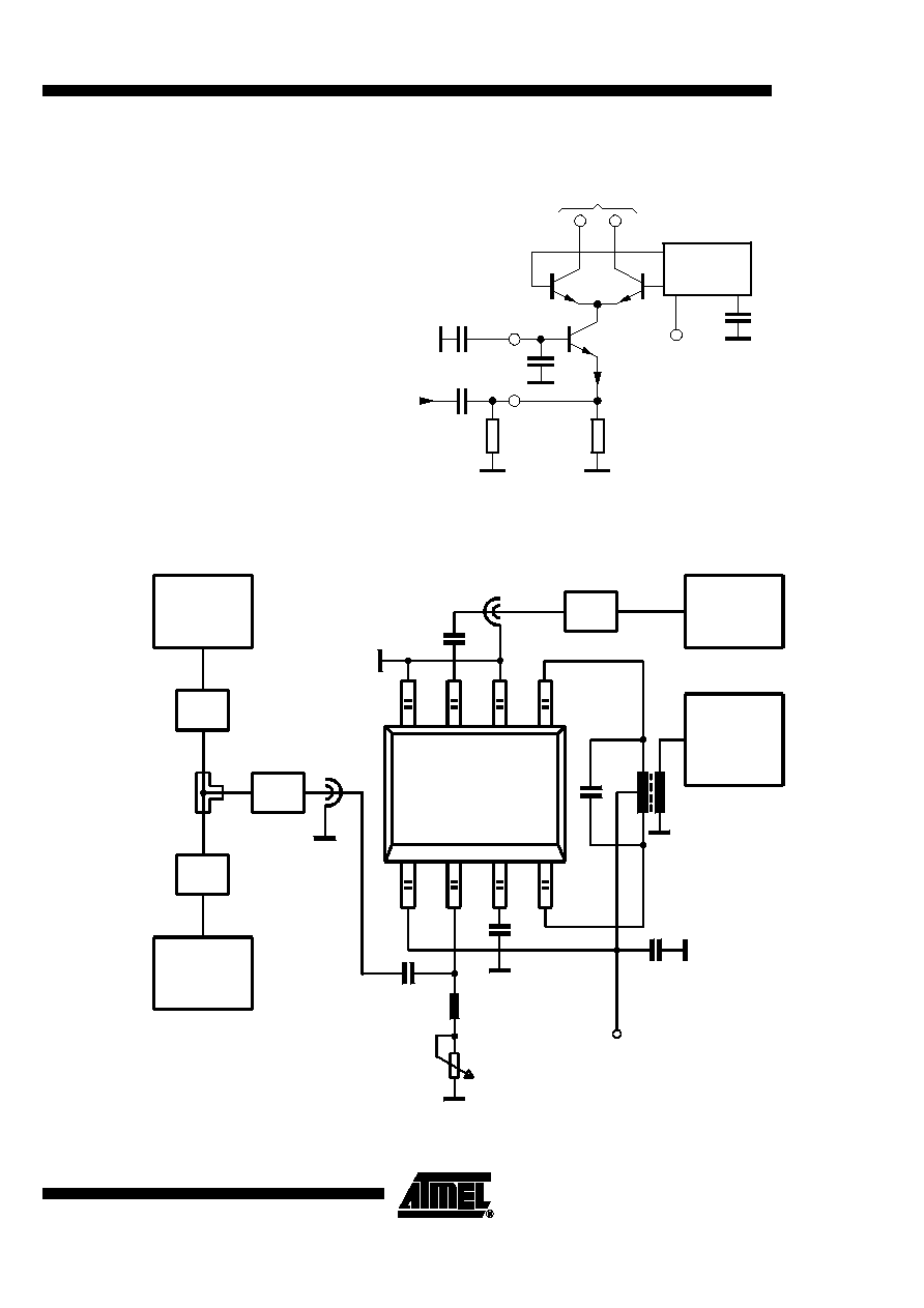
Figure 5. Mixer Circuitry
Figure 6. Test Circuit Conversion Power Gain (PG
C
) and 3rd-order Input Intercept Point (IIP3)
R
E
RF
I
LO Buffer
5
4
IF
O
7
LO
I
I
M
3
2
8
7
6
5
1
2
3
4
C2
3
C
IP3
R
1
Spectrum
analyzer
Hp 70908 A
R = 50
W
i
N
C4
1
C
LO
R = 50
W
i
10 dB
LOi
10 dB
i
1. RF
generator
R = 50
W
10 dB
10 dB
i
2. RF
R = 50
W
RFi
Power
splitter
V
S
r
C
U2796B
f
1
= 958.5 MHz
f = 900 MHz
LO
f = 958.55 MHz
2
-10 dBm
-26 dBm
m
H
IFO
IFO
generator
generator

