
Rev. 4735A≠RKE≠11/03
Features
∑
IC Distinguishes the Signal Strength of Several Transmitters via RSSI (Received Signal
Strength Indicator) Output
∑
Minimal External Circuitry Requirements, No RF Components on the PC Board Except
Matching to the Receiver Antenna
∑
High Sensitivity, Especially at Low Data Rates
∑
Sensitivity Reduction Possible Even While Receiving
∑
Fully Integrated VCO
∑
Low Power Consumption Due to Configurable Self-polling with a Programmable Time
Frame Check
∑
Supply Voltage 4.5 V to 5.5 V
∑
Operating Temperature Range -40
∞
C to 105
∞
C
∑
Single-ended RF Input for Easy Adaptation to
/4 Antenna or Printed Antenna on PCB
∑
Low-cost Solution Due to High Integration Level
∑
ESD Protection According to MIL-STD. 883 (4 KV HBM)
∑
High Image Frequency Suppression Due to 1 MHz IF in Conjunction with a SAW
Front-end Filter (Up to 40 dB Achievable with Newer SAWs)
∑
Communication to Microcontroller Possible via a Single, Bi-directional Data Line
∑
Power Management (Polling) is also Possible by Means of a Separate Pin via the
Microcontroller
Description
The U3742BM is a multi-chip PLL receiver device supplied in an SO20 package. It has
been especially developed for the demands of RF low-cost data transmission systems
with data rates from 1 kBaud to 10 kBaud (1 kBaud to 3.2 kBaud for FSK) in Manches-
ter or Bi-phase code. The receiver is well suited to operate with Atmel's PLL RF
transmitter IC U2741B. Its main applications in the area of wireless control are teleme-
tering, security technology, tire-pressure monitoring and keyless-entry systems. It can
be used in the frequency receiving range of f
0
= 300 MHz to 450 MHz for ASK or FSK
data transmission. All the statements made in this data sheet refer both to
433.92 MHz and 315 MHz applications.
UHF ASK/FSK
Receiver
U3742BM
2
U3742BM
4735A≠RKE≠11/03
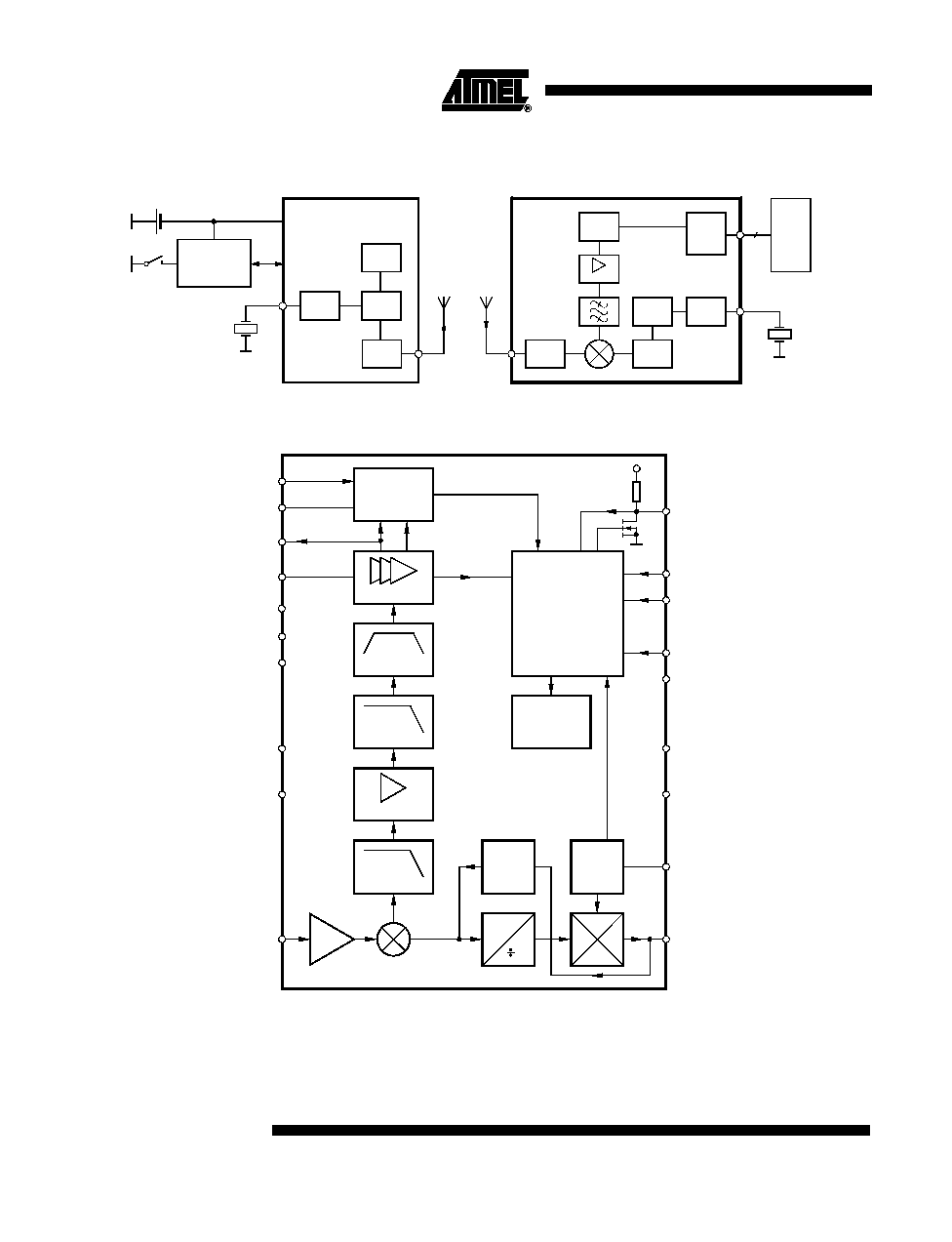
Figure 1. System Block Diagram
Figure 2. Block Diagram
Demod.
IF Amp
LNA
VCO
PLL
XTO
Control
U3742BM
1...3
Micr
o
-
cont
r
o
ller
Power
amp.
XTO
VCO
PLL
U2741B
Antenna Antenna
UHF ASK/FSK
Remote control transmitter
UHF ASK/FSK
Remote control receiver
Encoder
ATARx9x
1 Li cell
Keys
FSK/ASK-
Demodulator
and data filter
IF Amp
IF Amp
4. Order
LPF
3 MHz
LPF
3 MHz
Dem_out
Limiter out
RSSI
Sensitivity
reduction
Standby logic
Polling circuit
and
control logic
FE
CLK
VCO
XTO
64
f
50 k
V
S
FSK/ASK
CDEM
AVCC
SENS
AGND
DGND
MIXVCC
LNAGND
LNA_IN
DATA
ENABLE
TEST
MODE
LFGND
LFVCC
XTO
LF
DVCC
LNA
RSSI

3
U3742BM
4735A≠RKE≠11/03
Pin Configuration
Figure 3. Pinning SO20
1
2
3
4
5
6
7
8
10
9
19
18
17
16
14
15
13
12
11
20
AVCC
AGND
DGND
MIXVCC
LNAGND
LNA_IN
FSK/ASK
CDEM
RSSI
MODE
XTO
LFGND
LF
ENABLE
TEST
NC
LFVCC
DATA
DVCC
SENS
Pin Description
Pin
Symbol
Function
1
SENS
Sensitivity-control resistor
2
FSK/ASK
Selecting FSK/ASK
Low: FSK, High: ASK
3
CDEM
Lower cut-off frequency of the data filter
4
AVCC
Analog power supply
5
AGND
Analog ground
6
DGND
Digital ground
7
MIXVCC
Power supply mixer
8
LNAGND
High-frequency ground LNA and mixer
9
LNA_IN
RF input
10
NC
Not connected
11
LFVCC
Power supply VCO
12
LF
Loop filter
13
LFGND
Ground VCO
14
XTO
Crystal oscillator
15
DVCC
Digital power supply

4
U3742BM
4735A≠RKE≠11/03
RF Front End
The RF front end of the receiver is a heterodyne configuration that converts the input
signal into a 1 MHz IF signal. According to Figure 2 on page 2, the front end consists of
an LNA (low noise amplifier), LO (local oscillator), a mixer and an RF amplifier.
The LO generates the carrier frequency for the mixer via a PLL synthesizer. The XTO
(crystal oscillator) generates the reference frequency f
XTO
. The VCO (voltage-controlled
oscillator) generates the drive voltage frequency f
LO
for the mixer. f
LO
is dependent on
the voltage at pin LF. f
LO
is divided by a factor of 64. The divided frequency is compared
to f
XTO
by the phase frequency detector. The current output of the phase frequency
detector is connected to a passive loop filter and thereby generates the control voltage
V
LF
for the VCO. By means of that configuration, V
LF
is controlled in a way that f
LO
/64 is
equal to f
XTO
. If f
LO
is determined, f
XTO
can be calculated using the following formula:
f
XTO
= f
LO
/64
The XTO is a one-pin oscillator that operates at the series resonance of the quartz crys-
tal. According to Figure 4, the crystal should be connected to GND via the capacitor CL.
The value of that capacitor is recommended by the crystal supplier. The value of CL
should be optimized for the individual board layout to achieve the exact value of f
XTO
and
hereby of f
LO
. When designing the system in terms of receiving bandwidth, the accuracy
of the crystal and the XTO must be considered.
Figure 4. PLL Peripherals
16
MODE
Selecting 433.92 MHz/315 MHz
Low: 4.90625 MHz (USA)
High: 6.76438 (Europe)
17
RSSI
Output of the RSSI amplifier
18
TEST
Test pin, during operation at GND
19
ENABLE
Enables the polling mode
Low: polling mode off (sleep mode)
High: polling mode on (active mode)
20
DATA
Data output/configuration input
Pin Description (Continued)
Pin
Symbol
Function
DVCC
XTO
LF
LFVCC
LFGND
V
C
C
10
R
1
C
9
S
L
V
S
R
1
= 820
C
9
= 4.7 nF
C
10
= 1 nF

5
U3742BM
4735A≠RKE≠11/03
The passive loop filter connected to pin LF is designed for a loop bandwidth of
B
Loop
= 100 kHz. This value for B
Loop
exhibits the best possible noise performance of the
LO. Figure 4 on page 4 shows the appropriate loop filter components to achieve the
desired loop bandwidth. If the filter components are changed for any reason, please
note that the maximum capacitive load at pin LF is limited. If the capacitive load is
exceeded, a bit check may no longer be possible since f
LO
cannot settle in time before
the bit check starts to evaluate the incoming data stream. Self-polling does therefore
also not work in that case.
f
LO
is determined by the RF input frequency f
RF
and the IF frequency f
IF
using the follow-
ing formula:
f
LO
= f
RF
- f
IF
To determine f
LO
, the construction of the IF filter must be considered at this point. The
nominal IF frequency is f
IF
= 1 MHz. To achieve a good accuracy of the filter's corner fre-
quencies, the filter is tuned by the crystal frequency f
XTO
. This means that there is a
fixed relation between f
IF
and f
LO
, that depends on the logic level at pin MODE. This is
described by the following formulas:
The relation is designed to achieve the nominal IF frequency of f
IF
= 1 MHz for most
applications. For applications where f
RF
= 315 MHz, MODE must be set to '0'. In the
case of f
RF
= 433.92 MHz, MODE must be set to '1'. For other RF frequencies, f
IF
is not
equal to 1 MHz. f
IF
is then dependent on the logical level at pin MODE and on f
RF
. Table
1 on page 6 summarizes the different conditions.
The RF input either from an antenna or from a generator must be transformed to the RF
input pin LNA_IN. The input impedance of that pin is provided in the electrical parame-
ters. The parasitic board inductances and capacitances also influence the input
matching. The RF receiver U3742BM exhibits its highest sensitivity at the best signal-to-
noise ratio in the LNA. Hence, noise matching is the best choice for designing the trans-
formation network.
A good practice when designing the network is to start with power matching. From that
starting point, the values of the components can be varied to some extent to achieve the
best sensitivity.
If a SAW is implemented into the input network, a mirror frequency suppression of
D
P
Ref
= 40 dB can be achieved. There are SAWs available that exhibit a notch at
D
f = 2 MHz. These SAWs work best for an intermediate frequency of IF = 1 MHz. The
selectivity of the receiver is also improved by using a SAW. In typical automotive appli-
cations, a SAW is used.
Figure 5 on page 6 shows a typical input matching network for f
RF
= 315 MHz and
f
RF
= 433.92 MHz using a SAW. Figure 6 on page 6 illustrates input matching to 50
W
without a SAW. The input matching networks shown in Figure 6 on page 6 are the refer-
ence networks for the parameters given in the electrical characteristics.
MODE
0 (USA) f
IF
f
LO
314
----------
=
=
MODE
1 (Europe) f
IF
f
LO
432.92
------------------
=
=