 | –≠–ª–µ–∫—Ç—Ä–æ–Ω–Ω—ã–π –∫–æ–º–ø–æ–Ω–µ–Ω—Ç: U4037B-N | –°–∫–∞—á–∞—Ç—å:  PDF PDF  ZIP ZIP |

U4037B-N
Preliminary Information
Rev. A3, 06-Mar-01
1 (7)
mC-Controlled Speech and Ringer Circuit
Description
The
µ
C-controlled telephone circuit U4037B-N is a lin-
ear integrated circuit for use in telephone sets. It contains
the speech circuit, tone-ringer interface, sidetone equiva-
lent and ear-protection rectifiers. The circuit is line
powered and contains all components necessary for
amplification of signals and adaptation to the line.
Features
D DC characteristic adjustable
D Receive gain adjustable
D Symmetrical input of microphone amplifier
D Anti-clipping in transmit direction
D Automatic line-loss compensation
D Symmetrical output of earpiece amplifier
D Built-in ear protection
D DTMF and MUTE input
D Adjustable sidetone suppression independent
of sending and receiving amplification
D Power down
D Tone-ringer interface
D 2-bit D/A for volume control
D Supply voltages for all functional blocks of a
subscriber set
D Operation possible from 8-mA line currents
Benefits
D Complete system integration of analog signal
processing on one chip
D Very few external components
Applications
Telephone sets
Block Diagram
mC
Power
supply
Speech
circuit
Tone
ringer
PWR
14076
Ordering Information
Type
Package
Remarks
U4037B-NFL
SO24
U4037B-NFLG3
SO24
Taped and reeled
U4037B-N
Rev. A3, 06-Mar-01
Preliminary Information
2 (7)
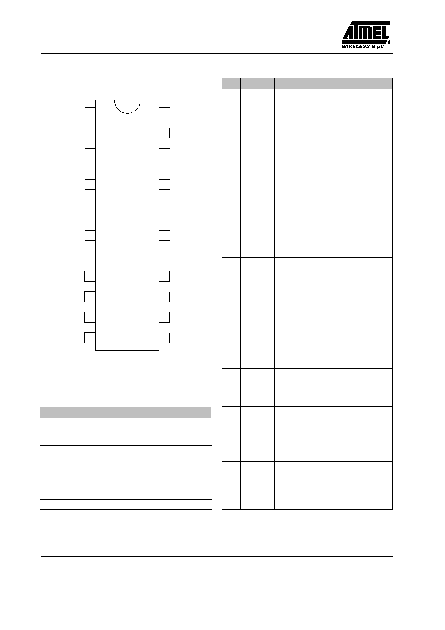
Pin Description
1
2
3
4
5
6
7
8
10
9
23
18
17
16
14
15
13
12
11
24
21
22
19
20
VOL1
MU/VOL2
16276
MEL
PD
VMP
VRING
AGA
DTMF
OUT2
TXACL
ST
MICO
RECIN
VB
IMP
GND
VL
IND
RECO1
RIF
OUT1
RECO2
MIC1
MIC2
Figure 1. Pinning
Pin
Symbol
Function
1
MICO
Output of microphone preamplifier
2
ST
Sidetone reduction input
input resistance is approx. 25 k
.
3
TXACL
Time constant of anti-clipping in
transmit path
4
AGA
Automatic gain adjustment with line
current, a resistor connected from
this pin to GND sets the starting
point maximum gain change: 6 dB.
5
DTMF
Input for DTMF signals
Pin
Symbol
Function
6
VOL1
2-bit volume adjustment for tone
ringer
7
MU/
VOL2
1. 2-bit volume adjustment for tone
ringer
2. Mute of microphone amplifier:
≠ Speech condition,
input MU/VOL2 low
≠ DTMF condition
input MU/VOL2 high
DTMF signal at Pin 5 is fed to
the line. A part of the DTMF-
signal is passed to the receiving
amplifier as a confidence signal
during dialing.
8
MEL
Input for melody
9
PD
Active high input for reducing the
current consumption of the circuit,
simultaneously V
L
is shorted by an
internal switch
10
VMP
Regulated supply voltage 3.4 V for
peripheral circuits (esp. micropro-
cessors), minimum output current:
2 mA (ringing) 4 mA (speech mode)
11
VRING
Input for ringersupply voltage
12
OUT2
Differential output for tone ringer
13
OUT1
Differential output for tone ringer
14
IND
The internal equivalent inductance
of the circuit is proportional to the
value of the capacitor at this pin, a
resistor connected to ground may be
used to reduce the DC line voltage
15
VL
Line voltage
16
GND
Reference point for DC- and AC-
output signals
17
IMP
Impedance adjustment
18
VB
Unregulated supply voltage for
peripheral circuits (voice switch),
limited to typically 7 V
19
RECIN
Receiver input
20
RIF
Pin for adjustment of frequency
response and gain of receiver
21
RECO1
Output of receiving amplifier
22
RECO2
Inverting output of receiving ampl.
23
MIC1
Inverting input of microphone ampl.
24
MIC2
Non-inverting input of microphone
amplifier

U4037B-N
Preliminary Information
Rev. A3, 06-Mar-01
3 (7)
Detailed Block Diagram with External Components
Power down
control
VMPREG1
MIC1
MIC2
VMP
DTMF
TXACL
TXACL
MICO
ST
RA
RECO1
RECO2
AGA
TXA
DC ≠ Mask
and
supply
AGA
PD
RECIN
VL
IMP
IND
GND
VRING
V
olume
control
BUZA
VMPREG2
OUT1
VOL1
MU/
MEL
VB
VMP
47
m
1000
m
to
m
C
Ti
p
Ring
m
C
VMP
16277
+
≠
RIF
OUT2
10k
4.7n
51k
5.6n
20k
1k
10k
15k
1k
12k
6.8n
6.8n
3.3n
1
m
23k
20k
560
100n
33n
50
50
33k
1n
220n
10
m
10
m
10
1M
16V
200k
130k
10
10n
12V
3.3M
*
*
*
*
*
*
*
*
*
*
*
V
alue depends on the application
VOL2
Figure 2. Application circuit

U4037B-N
Rev. A3, 06-Mar-01
Preliminary Information
4 (7)
Absolute Maximum Ratings
Parameters
Symbol
Value
Unit
¡¡¡¡¡¡¡¡¡¡¡¡¡¡¡¡¡
¡¡¡¡¡¡¡¡¡¡¡¡¡¡¡¡¡
Line current
¡¡¡¡
¡¡¡¡
I
L
¡¡¡¡¡¡¡¡¡
¡¡¡¡¡¡¡¡¡
140
¡¡¡¡¡
¡¡¡¡¡
mA
¡¡¡¡¡¡¡¡¡¡¡¡¡¡¡¡¡
¡¡¡¡¡¡¡¡¡¡¡¡¡¡¡¡¡
DC line voltage
¡¡¡¡
¡¡¡¡
V
L
¡¡¡¡¡¡¡¡¡
¡¡¡¡¡¡¡¡¡
12
¡¡¡¡¡
¡¡¡¡¡
V
¡¡¡¡¡¡¡¡¡¡¡¡¡¡¡¡¡
¡¡¡¡¡¡¡¡¡¡¡¡¡¡¡¡¡
Maximum input current
¡¡¡¡
¡¡¡¡
I
RING
¡¡¡¡¡¡¡¡¡
¡¡¡¡¡¡¡¡¡
15
¡¡¡¡¡
¡¡¡¡¡
mA
¡¡¡¡¡¡¡¡¡¡¡¡¡¡¡¡¡
¡¡¡¡¡¡¡¡¡¡¡¡¡¡¡¡¡
Junction temperature
¡¡¡¡
¡¡¡¡
T
j
¡¡¡¡¡¡¡¡¡
¡¡¡¡¡¡¡¡¡
125
¡¡¡¡¡
¡¡¡¡¡
∞
C
¡¡¡¡¡¡¡¡¡¡¡¡¡¡¡¡¡
¡¡¡¡¡¡¡¡¡¡¡¡¡¡¡¡¡
Ambient temperature
¡¡¡¡
¡¡¡¡
T
amb
¡¡¡¡¡¡¡¡¡
¡¡¡¡¡¡¡¡¡
≠25 to +75
¡¡¡¡¡
¡¡¡¡¡
∞
C
¡¡¡¡¡¡¡¡¡¡¡¡¡¡¡¡¡
¡¡¡¡¡¡¡¡¡¡¡¡¡¡¡¡¡
Storage temperature
¡¡¡¡
¡¡¡¡
T
stg
¡¡¡¡¡¡¡¡¡
¡¡¡¡¡¡¡¡¡
≠55 to +150
¡¡¡¡¡
¡¡¡¡¡
∞
C
¡¡¡¡¡¡¡¡¡¡¡¡¡¡¡¡¡
¡¡¡¡¡¡¡¡¡¡¡¡¡¡¡¡¡
Total power dissipation,
T
amb
= 60
∞
C
¡¡¡¡
¡¡¡¡
P
tot
¡¡¡¡¡¡¡¡¡
¡¡¡¡¡¡¡¡¡
520
¡¡¡¡¡
¡¡¡¡¡
W
Thermal Resistance
Parameters
Symbol
Value
Unit
Junction ambient
SO24
R
thJA
75
K/W
Electrical Characteristics
f = 1 kHz, 0 dBm = 775 mV
rms
, I
MP
= 2 mA, T
amb
= 25
∞
C, Z
ear
= 68 nF + 100
W, Z
M
= 68 nF, unless otherwise specified
Parameters
Test Conditions / Pin
Symbol
Min.
Typ.
Max.
Unit
DC characteristics
DC voltage drop over circuit
I
L
= 2 mA
I
L
= 14 mA
I
L
= 60 mA
I
L
= 100 mA
V
L
4.6
8.8
2.4
5.0
7.5
9.4
5.4
10.0
V
Transmission amplifier, I
L
= 14 mA, V
MIC
= 2 mV, unless otherwise specified
Transmitting amplification
G
T
47
48
49
dB
Frequency response
I
L
w 14 mA,
f = 300 to 3400 Hz
DG
T
"0.5
dB
Gain change with current
I
L
= 14 to 100 mA
DG
T
"0.5
dB
Gain deviation
T
amb
= ≠10 to +60
∞
C
DG
T
"0.5
dB
CMRR of microphone
amplifier
CMRR
60
80
dB
Input resistance of MIC amplifier
R
i
50
k
W
Distortion at line
I
L
> 14 mA
V
L
= 700 mV
rms
d
t
2
%
Maximum output voltage
I
L
> 19 mA, d < 5%
V
mic
= 10 mV
CTXA = 1
mF
V
Lmax
1.8
3
4.2
dBm
Noise at line psophometrically
weighted
I
L
> 14 mA
G
T
= 48 dB
no
≠80
≠72
dBmp
Anti-clipping attack time
release time
CTXA = 1
mF
each 3 dB overdrive
0.5
9
ms
Line-loss compensation
I
L
= 100 mA,
RAGA = 20 k
W
DG
TI
≠6.4
≠5.8
≠5.2
dB
Mute suppression
I
L
w 14 mA
G
TM
60
80
dB

U4037B-N
Preliminary Information
Rev. A3, 06-Mar-01
5 (7)
Electrical Characteristics (continued)
Parameters
Test Conditions / Pin
Symbol
Min.
Typ.
Max.
Unit
Receiving amplifier, I
L
= 14 mA, unless otherwise specified, V
GEN
= 300 mV
Receiving amplification
G
R
12
dB
Adjustment range
G
R
≠8
12
dB
Amplification of DTMF signal from
DTMF IN to RECO 1, 2
I
L
w 14 mA,
V
DTMF
= 8 mV
G
RM
14
20
dB
Frequency response
I
L
> 14 mA,
f = 300 to 3400 Hz
DG
RF
"0.5
dB
Gain change with current
I
L
= 14 to 100 mA
DG
R
"0.5
dB
Gain deviation
T
amb
= ≠10 to +60
∞
C
DG
R
"0.5
dB
Ear protection differential
I
L
w 14 mA
V
GEN
= 11 V
rms
EP
2.2
V
rms
MUTE suppression
I
L
w 14 mA
DG
R
60
dB
Output voltage d
v 2%
differential
I
L
= 14 mA
Z
ear
= 68 nF + 100
W
0.775
V
rms
Output voltage d
v 5%
differential
I
L
= 14 mA
Z
ear
= 68 nF + 100
W
RDC = infinite
1.2
V
rms
Receiving noise
psophometrically weighted
Z
ear
= 68 nF + 100
W
I
L
w 14 mA
ni
≠64
dBmp
Output resistance
each output against GND
Ro
40
W
Line-loss compensation
RAGA = 20 k
W,
I
L
= 100 mA
DG
RI
≠7.0
≠6.0
≠5.0
dB
Gain at low operating current
I
L
= 8 mA, I
MP
= 1 mA
I
M
= 300
mA
V
GEN
= 100 mV
RDC = 68 k
W
G
R
10.5
12
13.5
dB
DTMF-amplifier
test conditions: IMP = 2 mA
DTMF amplification
I
L
= 15 mA,
VDTMF = 8 mV
Mute active
G
D
40.7
41.7
42.7
dB
Gain deviaton
I
L
= 15 mA
T
amb
= ≠10 to +60
∞
C
G
D
"0.5
dB
Input resistance
RGT = 15 k
W
R
i
15
20
25
k
W
Distortion of DTMF signal
I
L
w 15 mA,
V
L
= 0 dBm
d
D
2
%
Gain deviation with current
I
L
= 15 to 100 mA
DGD
"0.5
dB
Supply voltages, V
mic
= 10 mV, T
amb
= ≠ 10 to + 60
∞
C
V
MP
I
L
= 8 mA,
RDC = 130 k
W
I
MP
= 1 mA
V
MP
3.1
3.4
3.6
V
Ringing part, I
VMP
= 1 mA
Maximum output voltage
V
RING
= 20 V
V
out
25
V
pp
Input impedance in speech mode
f = 300 Hz to 3400 Hz
I
L
> 15 mA,
V
TIP/RING
= 1.5 V
rms
R
i
50
k
W