
Rev. 4807A≠AUDR≠05/04
Features
∑
On-chip Control Functions are Available for System Gain Adjust
(dB Linear versus DC Current)
∑
Low Noise LO Design
∑
ESD Protected
Benefits
∑
All Front-end Functions of a High-performance FM Receiver Except the RF
Preamplifier are Integrated
∑
Improved Dynamic Range by High Current Double-balanced Mixer Design and a New
AGC Conception with 3 Loops On-chip
∑
Improved Blocking and Intermod Behavior Due to a Unique "Interference" Sensor
Controlling the AGC
∑
Easy Cascading of 3 IF Filters (Ceramic) Enabled by Two On-chip IF Preamplifiers
Description
The IC U4065B is a bipolar integrated FM front-end circuit. It contains a mixer, an
oscillator, two IF preamplifiers and an unique interference sensor. The device is
designed for high-performance car radio and home receiver applications.
FM Receiver IC
U4065B

2
U4065B
4807A≠AUDR≠05/04
Figure 1. Block Diagram
V
S
22
1
11
9
8
10
6
17
13
3
5
7
4
21
18
19
16
14
23
24
+
IF BPF
IF BPF
IF BPF
IF output
IF 2
IF 1
IF gain adjust
V
S
Voltage
regulator
IF BPF
ANT
Interference
mixer
Mixer
RF
PIN
ATT
RF tank
V
TUNE
RF tank
Local
oscillator
IF tank
LO output
V
REF
= 4 V
20
2
LO tank
AGC adjust
AGC level
V
S
12
NC
(wide band)
AGC
wide band
and IF
IF and
detector
Interference
V
S
3
U4065B
4807A≠AUDR≠05/04
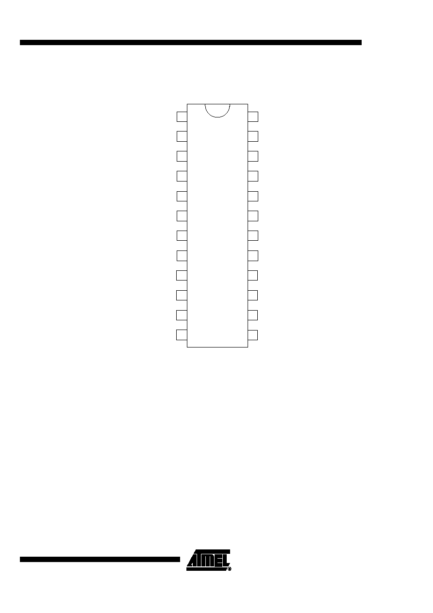
Pin Configuration
Figure 2. Pinning SO24
1
2
3
4
5
6
7
8
10
9
23
18
17
16
14
15
13
12
11
24
21
22
19
20
VS
IF1OUT
GND2
IMIFIN
AGCOUT
IMMIXOUT
GAINIF1
IF2IN
NC
IF2OUT
GND1
LOBUFF
MIXOUT2
MIXOUT1
VREF
MIXIN2
MIXIN1
GND3
IF1IN
GND4
AGCWB
GND5
LOE
LOB

4
U4065B
4807A≠AUDR≠05/04
Pin Description
Pin
Symbol
Function
1
LOBUFF
Buffered local oscillator output
2
GND1
Ground of the second IF amplifier
3
IF2OUT
Output of the second IF amplifier
4
GAINIF1
Gain control of the first IF amplifier
5
IF2IN
Input of the second IF amplifier
6
VS
Supply voltage
7
IF1OUT
Output of the first IF amplifier
8
GND2
Ground
9
IMIFIN
Input of the amplifier for the IM sensor
10
AGCOUT
Output of the automatic gain control
11
IMMIXOUT
Output of the intermodulation mixer
12
NC
Not connected
13
AGCWB
Threshold adjustment of the wideband AGC
14
GND3
Mixer ground
15
MIXIN1
Input 1 of the double-balanced mixer
16
MIXIN2
Input 2 of the double-balanced mixer
17
VREF
Reference voltage output
18
MIXOUT1
Mixer output 1
19
MIXOUT2
Mixer output 2
20
GND4
Ground of the first IF amplifier
21
IF1IN
Input of the first IF amplifier
22
GND5
Oscillator ground
23
LOE
Local oscillator (emitter)
24
LOB
Local oscillator (base)

5
U4065B
4807A≠AUDR≠05/04
LOBUFF
Figure 3. Buffered Local Oscillator Output
The buffered local oscillator used for output, drives the FM input of the PLL circuit (for
example, U428xBM family). The typical parallel output resistance at 100 MHz is 70
,
the parallel output capacitance is about 10 pF. When using an external load of 500
/10
pF, the oscillator swing is about 100 mV. The second harmonic of the oscillator fre-
quency is less than -15 dBc.
GND1
Figure 4. Ground of the Second IF Amplifier
There is no internal connection to the other ground pins.
IF2OUT
Figure 5. Output of the Second IF Amplifier
The parallel output capacitance to ground is about 7 pF. The external load resistance
must be connected to V
S
. The DC current into the pin is typically 3 mA.
Note:
The supply voltage V
S
has to be protected against IF distortion.
ESD
50
23
1
+
1 V
ESD
8
2
ESD
3
V
S
V
REF