 | –≠–ª–µ–∫—Ç—Ä–æ–Ω–Ω—ã–π –∫–æ–º–ø–æ–Ω–µ–Ω—Ç: U4082B | –°–∫–∞—á–∞—Ç—å:  PDF PDF  ZIP ZIP |
U4082B
Rev. A2, 12-Feb-01
1 (22)
Low-Voltage Voice-Switched IC for Hands-Free Operation
Description
The low-voltage voice-switched speakerphone circuit,
U4082B, incorporates the wide range of functions listed
below. Versatility of the device is further enhanced by
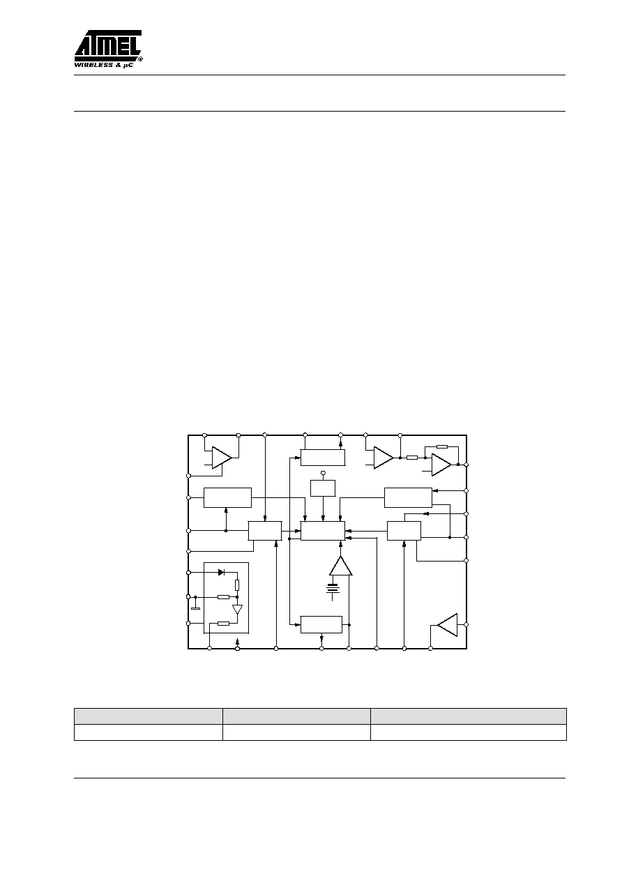
giving access to internal circuit points. The block diagram
(figure 1) shows amplifiers, level detectors, transmit and
receive attenuators operating in complementary func-
tions, background noise monitors, chip disable, dial tone
detector and mute function. Due to low-voltage opera-
tion, it can be operated either by a low supply or via a
telephone line requiring 5.5 mA typically. Also featured
is stand-alone operation through a coupling transformer
(Tip and Ring) or in conjunction with a handset speech
network, as shown in figure 2.
Features
D Low-voltage operation: 3 to 6.5 V
D Attenuator gain range between transmit and
receive: 52 dB
D Four point signal sensing for improved sensitivity
D Monitoring system for background-noise level
D Microphone amplifier gain adjustable
D Mute function
D Chip disable for active/standby operation
D On-board filter
D Dial tone detector
D Compatible with U4083B speaker amplifier
Benefits
D Fast channel switching allows quasi duplex operation
D Proper operation in noisy surrounding
Block Diagram
10
B
V
11
12
16
Level
detectors
18
19
4
28
3
400
W
15
14
17
Attenuator
control
AGC
T-attenuator
≠
+
S
V
9
8
7
≠
+
B
V
6
≠
+
B
V
B
V
Dial tone
detector
20
22
21
5
27
23
25
24
+ ≠
13
26
1
2
+1
Filter
93 7766 e
R-attenuator
U 4082 B
Background
noise monitor
Background
noise monitor
Level
detectors
PD
HTO+
HTO≠
CD
HTI
FI
TLI2
V
S
CPT
RI
VCI
MIC
MUTE
MICO
TI
TO
C
T
V
B
TLI1
RLI2 RECO
RLO1
GND
RLO2
TLO1
RLI1
TLO2
CPR
Figure 1. Block diagram
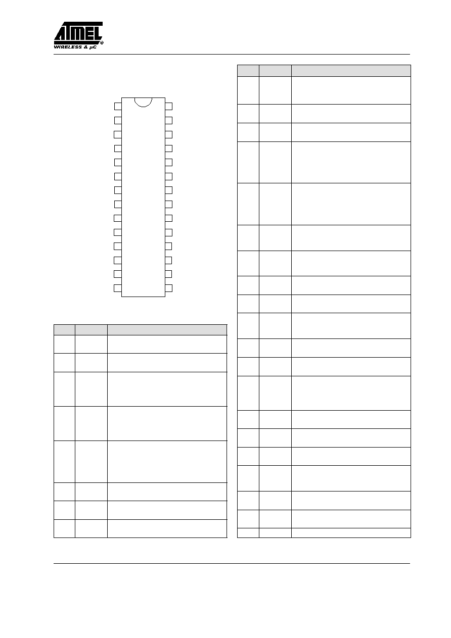
Ordering Information
Extended Type Number
Package
Remarks
U4082B≠MFL
SO28
Taped and reeled

U4082B
Rev. A2, 12-Feb-01
2 (22)
k
W
MICO
1
0
B
V
11
MI
C
Background
noise monitor
MUTE
12
16
CP
T
100 k
W
47
18
2
19
TL
O
2
RL
O
2
2
4
S
V
28
GND
1000
3
CD
400
W
15
1
4
B
V
T
C
180 k
W
TL
I
2
17
0.1
270 pF
B
V
20
620
W
0.
2
5.1 k
5.1 k
W
1
0.02
S
V
5.1 V
1N4733
Attenuator
control
AGC
T≠ attenuator
≠
+
S
V
10
k
W
TI
9
T
O
8H
T
I
7
≠
+
B
V
0.1
51 k
W
6
≠
+
B
V
B
V
Dial tone
detector
RL
I
2
2
0
RE
C
O
2
2
R
I
2
1
V
C
I
Level
detector
Background
noise monitor
5
HT
O
+
27
CP
R
23
TL
I
1
25
RL
O
1
24
TL
O
1
820
W
300
W
0.05
0.1
5.1 k
W
Balancing
network
0.01
Hook
switch
100 k
W
47
Ti
p
Ring
S
V
2
2
12
0
k
W
22
0
5
+
+
≠
≠
6
13
7
4
8
5
0.05
10 k
W
1
10 k
W
200 pF
+≠
13
RL
I
1
2
6
FO
1
2
FI
+1
Filter
0.05
10 k
W
56 k
W
0.1
20 k
W
V
olume control
B
V
B
V
220 k
W
4700 pF
4700 pF
937734 e
HT
O ≠
R≠ attenuator
5.1 k
W
9.1 k
W
W
m
F
m
F
m
F
m
F
m
F
m
F
m
F
m
F
m
F
m
F
m
F
m
F
m
F
m
F
m
F
m
F
m
F
m
F
m
F
m
F
m
F
m
F
Level
detector
0.1
0.1
U4082B
U4083B
Figure 2. Block diagram with external circuit
U4082B
Rev. A2, 12-Feb-01
3 (22)
Pin Description
1
2
3
4
5
6
7
8
10
9
27
22
21
20
18
19
17
12
11
28
25
26
23
24
HTO≠
HTI
TO
TI
MICO
MIC
VS
HTO+
MUTE
CD
FI
FO
TLI1
RECO
RI
RLI2
RLO2
TLO2
RLO1
TLO1
TLI2
RLI1
CPR
GND
16
15
14
13
VCI
CT
CPT
VB
Pin
Symbol
Function
1
FO
Filter output. Output impedance is less
than 50
W.
2
FI
Filter input. Input impedance is greater
than 1 M
W.
3
CD
Chip disable. A logic low (< 0.8 V) sets
normal operation. A logic high (> 2 V)
disables the IC to conserve power. Input
impedance is nominally 90 k
W.
4
V
S
Supply voltage 2.8 to 6.5 V, approxi-
mately 5 mA. AGC circuit reduces the
receive attenuator gain @ 25 dB
* Re-
ceive mode at 2.8 V.
5
HTO+
Output of the second hybrid amplifier.
*
Hybrid output. Gain is internally set at ≠1
to provide a differential output, (in con-
junction with HTO≠) to the hybrid trans-
former.
6
HTO≠
Output of the first hybrid amplifier. Hy-
brid output. Gain is set by ext. resistors.
7
HTI
Input and summing node for the first hy-
brid amplifier. DC level is approx. V
B
.
8
TO
Transmit attenuator output.
DC level is approximately V
B
.
Pin
Symbol
Function
9
TI
Transmit attenuator input. Maximum sig-
nal level is 350 mVrms. Input impedance
is approximately 10 k
W
10
MICO
Microphone amplifier output.
Gain is set by external resistors.
11
MIC
Microphone amplifier input. Bias voltage
is approximately V
B
.
12
MUTE
Mute input. A logic low (< 0.8 V) sets
normal operation. A logic high (> 2 V)
mutes the microphone amplifier without
affecting the rest of the circuit. Input
impedance is nominally 90 k
W.
13
VCI
Volume control input. When VCI = V
B
,
the receive attenuator is at maximum gain
when in receive mode. When VCI = 0.3
V
B
, the receive gain is down 35 dB. It
does not affect the transmit mode.
14
C
T
Response time.
An RC at this pin sets the response time
for the circuit to switch modes.
15
V
B
Output voltage
[ V
S/2
. It is a system ac
ground and biases the volume control. A
filter cap is required.
16
CPT
An RC at this pin sets the time constant
for the transmit background monitor.
17
TLI2
Transmit level detector input on the mi-
crophone/speaker side.
18
TLO2
Transmit level detector output on the mi-
crophone/speaker side, and input to the
transmit background monitor.
19
RLO2
Receive level detector output on the mi-
crophone/speaker side.
20
RLI2
Receive level detector input on the micro-
phone/speaker side.
21
RI
Input receive attenuator and dial tone de-
tector. Maximum input level is
350 mVrms. Input impedance is approxi-
mately 10 k
W.
22
RECO
Receive attenuator output.
DC level is approximately V
B
.
23
TLI1
Transmit level detector input on the line
side.
24
TLO1
Transmit level detector output on the line
side.
25
RLO1
Receive level detector output on the line
side and input to the receive background
monitor.
26
RLI1
Receive level detector input on the line
side.
27
CPR
An RC at this pin sets the time constant
for the receive background monitor.
28
GND
Ground

U4082B
Rev. A2, 12-Feb-01
4 (22)
Introduction
General
The fundamental difference between the operation of a
speakerphone and a handset is that of half-duplex versus
full duplex. The handset is full duplex since conversation
can occur in both directions (transmit and receive)
simultaneously. A speakerphone has higher gain levels in
both paths, and attempting to converse full duplex results
in oscillatory problems due to the loop that exists within
the system. The loop is formed by the receive and transmit
paths, the hybrid and the acoustic coupling (speaker to
microphone).
The only practical and economical solution used to date
is to design the speakerphone to function in a half duplex
mode. That is, only one person speaks at a time, while the
other listens. To achieve this, a circuit is required which
can detect who is talking, switch on the appropriate path
(transmit or receive), and switch off (attenuate) the other
path. In this way, the loop gain is maintained less than
unity. When the talkers exchange function, the circuit
must quickly detect this, and switch the circuit
appropriately. By providing speech level detectors, the
circuit operates in a "hands-free" mode, eliminating the
need for a "push-to-talk" switch.
The handset has the same loop as the speakerphone.
Oscillations don't occur because the gains are
considerably lower and the coupling from the earpiece to
the mouthpiece is almost nonexistent (the receiver is
normally held against a person's ear).
The U4082B provides the necessary level detectors,
attenuators, and switching control for a properly
operating speakerphone. The detection sensitivity and
timing are externally controllable. Additionally, the
U4082B provides background noise monitors (which
make the circuit insensitive to room and line noise),
hybrid amplifiers for interfacing to tip and ring, the
microphone amplifier, and other associated functions.
For further explanation which is given below, please refer
to figure 1.
Transmit and Receive Attenuators TI, TO
and RI, RECO
The attenuators are complementary in function, i.e.,
when one is at maximum gain (+6.0 dB), the other is at
maximum attenuation (≠46 dB), and vice versa. Neither
is ever fully on or off. The sum of their gains remains
constant (within a nominal error band of
"0.1 dB) at a
typical value of ≠40 dB (see figure 11). Their purpose is
to control the transmit and receive paths to provide the
half-duplex operation required in a speakerphone.
The attenuators are non-inverting, and have a ≠3.0 dB
(from max. gain) frequency of approximately 100 kHz.
The input impedance of each attenuator (TI and RI) is
nominally 10 k
W (see figure 3), and to prevent distortion,
the input signal should be limited to 350 mVrms.
Maximum recommended input signal is independent of
the volume control setting. The diode clamp on the inputs
limits the input swing, and therefore the maximum
negative output swing. This is the reason V
RECO
and
V
TOL
specification are defined as they are in the electrical
characteristics. The output impedance is less than 10
W
until the output current limit (typically 2.5 mA) is
reached.
11 k
W
5 k
W
95 k
W
V
B
RI 21
TI 9
93 7740 e
to Attenuato
Input
Figure 3. Attenuator input stage
The attenuators are controlled by the single output of the
control block, which is measurable at the C
T
pin (Pin 14).
When the C
T
pin is at +240 mV w. r. t. V
B
, the circuit is
in the receive mode (receive attenuator is at +6.0 dB).
When the C
T
pin is at ≠240 mV w.r.t. V
B
, the circuit is in
the transmit mode (transmit attenuator is at +6.0 dB). The
circuit is in an idle mode when the C
T
voltage is equal to
V
B
causing the attenuators' gain to be halfway between
their fully on and fully off positions (≠20 dB each).
Monitoring the C
T
voltage (w.r.t. V
B
) is the most direct
method of monitoring the circuit's mode.
The attenuator control has seven inputs: two from the
comparators operated by the level detectors, two from the
background noise monitors, volume control, dial-tone
detector, and AGC. They are described as follows:

U4082B
Rev. A2, 12-Feb-01
5 (22)
Level Detectors
There are four level detectors, two on the receive side and
two on the transmit side. As shown in figure 4, the terms
in parentheses form one system, and the other terms form
the second system. Each level detector is a high-gain
amplifier with back-to-back diodes in the feedback path,
resulting in nonlinear gain, which permits operation over
a wide dynamic range of speech levels. Refer to the
graphs of figures 12, 13 and 14 for their DC and ac
transfer characteristics. The sensitivity of each level
detector is determined by the external resistor and
capacitor at each input (TLI1, TLI2, RLI1, and RLI2).
Each output charges an external capacitor through a diode
and limiting resistor, thus providing a DC representation
of the input ac signal level. The outputs have a quick rise
time (determined by the capacitor and an internal 350-
W
resistor) and a slow decay time set by an internal current
source and the capacitor. The capacitors on the four
outputs should have the same value (
"10%) to prevent
timing problems.
Referring to figure 2, on the receive side, one level
detector (RLI1) is at the receive input receiving the same
signal as at tip and ring, and the other (RLI2) is at the
output of the speaker amplifier. On the transmit side, one
level detector (TLI2) is at the output of the microphone
amplifier, while the other (TLI1) is at the hybrid output.
Outputs RLO1 and TLO1 feed a comparator. The output
of the comparator goes to the attenuator control block.
Likewise, outputs RLO2 and TLO2 feed a second
comparator which also goes to the attenuator control
block. The truth table for the effects of the level detectors
is given below in the attenuator control block section.
Background Noise Monitors
This circuit distinguishes speech (which consists of
bursts) from background noise (a relatively constant
signal level). There are two background noise monitors ≠
one for the receive path and the other for the transmit path.
The receive background noise monitor is operated on by
the RLI1-RLO1 level detector, while the transmit
background noise monitor is operated on by the
TLI2-TLO2 level detector (see figure 4).
They monitor the background noise by storing a DC
voltage representative of the respective noise levels in
capacitors at CPR and CPT. The voltages at these pins
have slow rise times (determined by the external RC), but
fast decay times. If the signal at RLI1 (or TLI2) changes
slowly, the voltage at CPR (or CPT) will remain more
positive than the voltage at the non-inverting input of the
monitor 's output comparator. When speech is present, the
voltage on the non-inverting input of the comparator will
rise quicker than the voltage at the inverting input (due to
the burst characteristic of speech), causing its output to
change. This output is sensed by the attenuator control
block.
V
B
V
≠
+
(TLI2) RLI1
(17) 26
5.1 k
W
0.1
mF
350
W
Level detector
(TLO2) RLO1
56 k
W
33 k
W
15
B
V
+
≠
≠
≠
+
+
36 mV
≠
+
350
W
Signal input
4
mA
B
V
5.1 k
W
0.1
mF
Signal input
Level detector
Background noise monitor
(RLI2) TLI1
(20) 23
TLO1
24
(19)
To attenuator
control block
≠
+
Comparator
C2 (C1)
C4 (C3)
(CPT)
CPR
27
(16) 100 k
W
S
93 7741 e
(18)25
2
mF
4
mA
47
mF
2
mF
(RLO2)
Figure 4. Level detectors