1
Features
∑
Wide Operating Voltage Range: 2 V to 16 V
∑
Low Current Consumption: 2.7 mA Typically
∑
Chip Disable Input to Power-down the Integrated Circuit
∑
Low Power-down Quiescent Current
∑
Drives a Wide Range of Speaker Loads
∑
Output Power P
o
= 250 mW at R
L
= 32
W
(Speaker)
∑
Low Harmonic Distortion (0.5% Typically)
∑
Wide Gain Range: 0 dB to 46 dB
Benefits
∑
Low Number of External Components
∑
Low Current Consumption
Description
The integrated circuit U4083B is a low-power audio amplifier for telephone loudspeak-
ers. It has differential speaker outputs to maximize the output swing at low supply
voltages. There is no need for coupler capacitors. The U4083B has an open loop gain
of 80 dB where the closed loop gain is adjusted with two external resistors. A chip dis-
able pin permits powering down and/or muting the input signal.
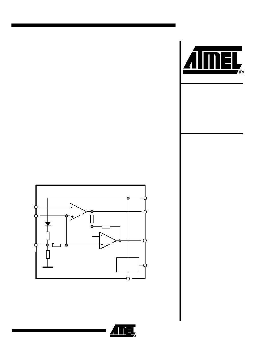
Figure 1. Block Diagram
Bias circuit
U4083B
4k 4k
50k
50k
125k
4
3
2
7
1
8
5
6
Amp1
Amp2
FC2
FC3
Vi
VS
VO1
VO2
CD
GND
Low-power
Audio Amplifier
for Telephone
Applications
U4083B
Rev. 4655A≠CORD≠01/03
3
U4083B
4655A≠CORD≠01/03
Functional Description Including External Circuitry
Pin 1: Chip Disable Digital
Input (CD)
Pin 1 (chip disable) is used to power down the IC to conserve power or muting or both.
Input impedance at Pin 1 is typically 90 k
W
.
∑
Logic 0 < 0.8 V
IC enabled (normal operation)
∑
Logic 1 > 2 V
IC disabled
Figure 17 shows the power supply current diagram. The change in differential gain from
normal operation to muted operation (muting) is more than 70 dB.
Switching characteristics are as follows:
∑
turn-on time
t
on
= 12 to 15 ms
∑
turn-off time
t
off
£
2 µs
They are independent of C
1
, C
2
and V
S
.
Voltages at Pins 2 and 3 are supplied from V
S
and therefore, do not change when the
U4083B is disabled. The outputs -- V
O1
(Pin 5) and V
O2
(Pin 8) -- turn to a high imped-
ance condition by removing the signal from the speaker.
When signals are applied from an external source to the outputs (disabled), they must
not exceed the range between the supply voltage, V
S
, and ground.
Pins 2 and 3: Filtering, Power
Supply Rejection
Power supply rejection is provided by capacitors C
1
and C
2
at Pin 3 and Pin 2, respec-
tively. C
1
is dominant at high frequencies whereas C
2
is dominant at low frequencies
(Figure 6 to Figure 9). The values of C
1
and C
2
depend on the conditions of each appli-
cation. For example, a line-powered speakerphone (telephone amplifier) will require
more filtering than a system powered by regulated power supply.
The amount of rejection is a function of the capacitors and the equivalent impedance at
Pin 3 and Pin 2 (see electrical characteristic equivalent resistance, R).
Apart from filtering, capacitors C
1
and C
2
also influence the turn-on time of the circuit at
power-up since capacitors are charged up through the internal resistors (50 k
W
and
125 k
W
) as shown in the block diagram.
Figure 3 shows the turn-on time versus C
2
at V
S
= 6 V, for two different C
1
values.
The turn-on time is 60% longer when V
S
= 3 V and 20% shorter when V
S
= 9 V.
The turn-off time is less than 10 µs.
Pin 4: Amplifier Input V
i
Pin 5: Amplifier Output 1 V
O1
Pin 8: Amplifier Output 2 V
O2
There are two identical operational amplifiers. Amplifier 1 has an open-loop gain
≥
80 dB at 100 Hz (Figure 4), whereas the closed-loop gain is set by external resistors, R
f
and R
i
(Figure 5). The amplifier is unity gain stable, and has a unity gain frequency of
approximately 1.5 MHz. A closed-loop gain of 46 dB is recommended for a frequency
range of 300 Hz to 3400 Hz (voice band). Amplifier 2 is internally set to a gain of -1.0 dB
(0 dB). The outputs of both amplifiers are capable of sourcing and sinking a peak cur-
rent of 200 mA. Output voltage swing is between 0.4 V and V
S
- 1.3 V at maximum
current (Figure 20 and Figure 21).
The output dc offset voltage between Pins 5 and 8 (V
O1
- V
O2
) is mainly a function of the
feedback resistor, R
f
, because the input offset voltages of the two amplifiers neutralize
each other.
Bias current of Amplifier 1 which is constant with respect to V
s
, flows out of Pin 4 (V
i
)
and through R
f
, forcing V
01
to shift negative by an amount equal to R
f
I
IB
and V
O2
positive
to an equal amount.

4
U4083B
4655A≠CORD≠01/03
The output offset voltage specified in the electrical characteristics is measured with the
feedback resistor (R
f
= 75 k
W
) shown in typical application circuit, Figure 22. It takes into
account the bias current as well as internal offset voltages of the amplifiers.
Pin 6: Supply and Power
Dissipation
Power dissipation is shown in Figure 10 to Figure 12 for different loads. Distortion char-
acteristics are given in Figure 13 to Figure 15.
where
T
jmax
= Junction temperature = 140∞C
T
amb
= Ambient temperature
R
thJA
= Thermal resistance, junction-ambient
Power dissipated within the IC in a given application is found from the following
equation:
P
tot
= (V
S
¥
I
S
) + (I
RMS
¥
V
S
) - (R
L
¥
I
RMS
2
)
I
S
is obtained from Figure 17.
I
RMS
is the RMS current at the load R
L
.
The IC's operating range is defined by a peak operating load current of ±200 mA (Figure
10 to Figure 15). It is further specified with respect to different loads (see Figure 16).
The left (ascending) portion of each of the three curves is defined by the power level at
which 10% distortion occurs. The center flat portion of each curve is defined by the max-
imum output current capability of the integrated circuit. The right (descending) portion of
each curve is defined by the maximum internal power dissipation of the IC at 25∞C. At
higher ambient temperatures, the maximum load power must be reduced according to
the above mentioned equation.
Layout Considerations
Normally, a snubber is not needed at the output of the IC, unlike many other audio
amplifiers. However, the PC board layout, stray capacitances, and the manner in which
the speaker wires are configured, may dictate otherwise. Generally, the speaker wires
should be twisted tightly, and be not more than a few cm (or inches) in length.
P
totmax
T
jmax
T
amb
≠
R
thJA
---------------------------------
=
5
U4083B
4655A≠CORD≠01/03
Absolute Maximum Ratings
Reference point Pin 7, T
amb
= 25
∞
C unless otherwise specified.
Parameters
Symbol
Value
Unit
Supply voltage
Pin 6
V
S
-1.0 to +18
V
Voltages
Disabled
Pins 1, 2, 3 and 4
Pins 5 and 8
-1.0 to (V
S
+1.0)
-1.0 to (V
S
+1.0)
V
V
Output current
Pins 5 and 8
±250
mA
Junction temperature
T
j
+140
∞
C
Storage temperature range
T
stg
-55 to +150
∞
C
Ambient temperature range
T
amb
-20 to +70
∞
C
Power dissipation SO8: T
amb
= 60
∞
C
P
tot
440
mW
Thermal Resistance
Parameters
Symbol
Value
Unit
Junction ambient
SO8
R
thJA
180
K/W
Operation Recommendation
Parameters
Symbol
Value
Unit
Supply voltage
Pin 6
V
S
2 to 16
V
Load impedance
Pins 5 to 8
R
L
8.0 to 100
W
Load current
I
L
± 200
mA
Differential gain (5.0 kHz bandwidth)
D
G
0 to 46
dB
Voltage at CD Pin 1
V
CD
V
S
V
Ambient temperature range
T
amb
-20 to +70
∞
C
Electrical Characteristics
T
amb
= +25
∞
C, reference point Pin 7, unless otherwise specified
Parameters
Test Conditions
Symbol
Min.
Typ.
Max.
Unit
Amplifiers (AC Characteristics)
Open-loop gain
(Amplifier 1, f < 100 Hz)
G
VOL1
80
dB
Closed-loop gain (Amplifier 2)
V
S
= 6.0 V, f = 1.0 kHz, R
L
= 32
W
G
V2
-0.35
0
+0.35
dB
Gain bandwidth product
G
BW
1.5
MHz
Output power
V
S
= 3.0 V, R
L
= 16
W
, d < 10%
V
S
= 6.0 V, R
L
= 32
W
, d < 10%
V
S
= 12 V, R
L
= 100
W
, d < 10%
Po
Po
Po
55
250
400
mW
Total harmonic distortion
(f = 1.0 kHz)
V
S
= 6.0 V, R
L
= 32
W
,
P
o
= 125 mW
V
S
> 3.0 V, R
L
= 8
W
,
P
o
= 20 mW
V
S
> 12 V, R
L
= 32
W
,
P
o
= 200 mW
d
d
d
0.5
0.5
0.6
1.0
%
