Rev. 4772B≠AUDR≠11/03
Features
∑
High Dynamic Range for AM and FM
∑
Integrated AGC for FM
∑
High Intercept Point 3rd-order for FM
∑
FM Amplifier Adjustable to Various Cable Impedances
∑
High Intercept Point 2nd-order for AM
∑
Low-noise Output Voltage
∑
Low-power Consumption
Electrostatic sensitive device.
Observe precautions for handling.
Description
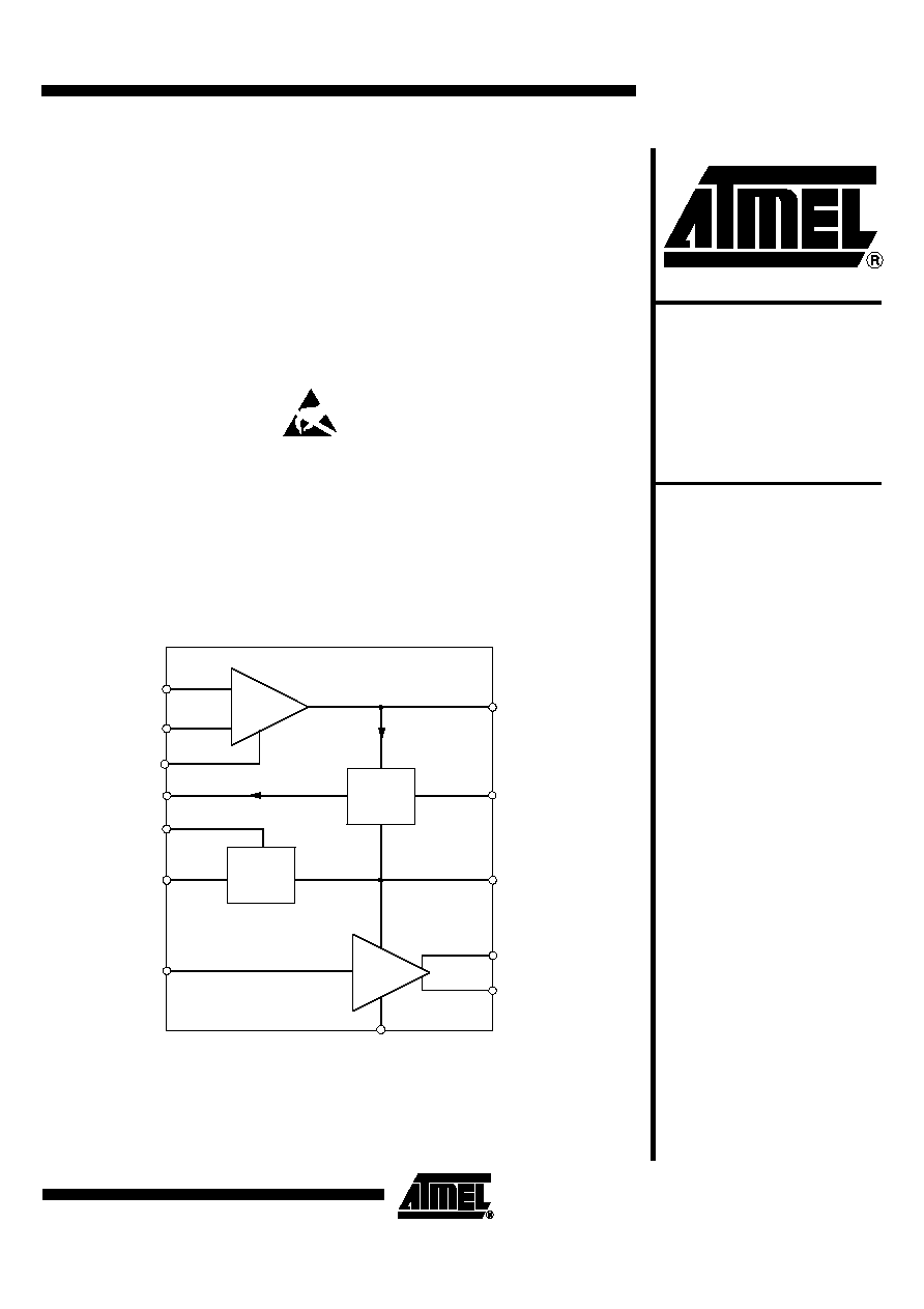
The U4254BM-M is an integrated low-noise AM/FM antenna impedance matching cir-
cuit in BiCMOS technology. The device is designed specifically for car applications
and is suitable for windshield and roof antennas.
Figure 1. Block Diagram
FM
AGC
FMIN
AGC
VS
AMIN
AMOUT
VREF1
FMOUT
FMGAIN
GND1
I
AGC
AGCADJ
GND2
VREF2
VREF
1
2
4
3
5
7
8
10
14
12
13
15
AMOUT1
11
AM
Low-noise
AM/FM Antenna
Impedance
Matching IC
U4254BM-M
2
U4254BM-M
4772B≠AUDR≠11/03
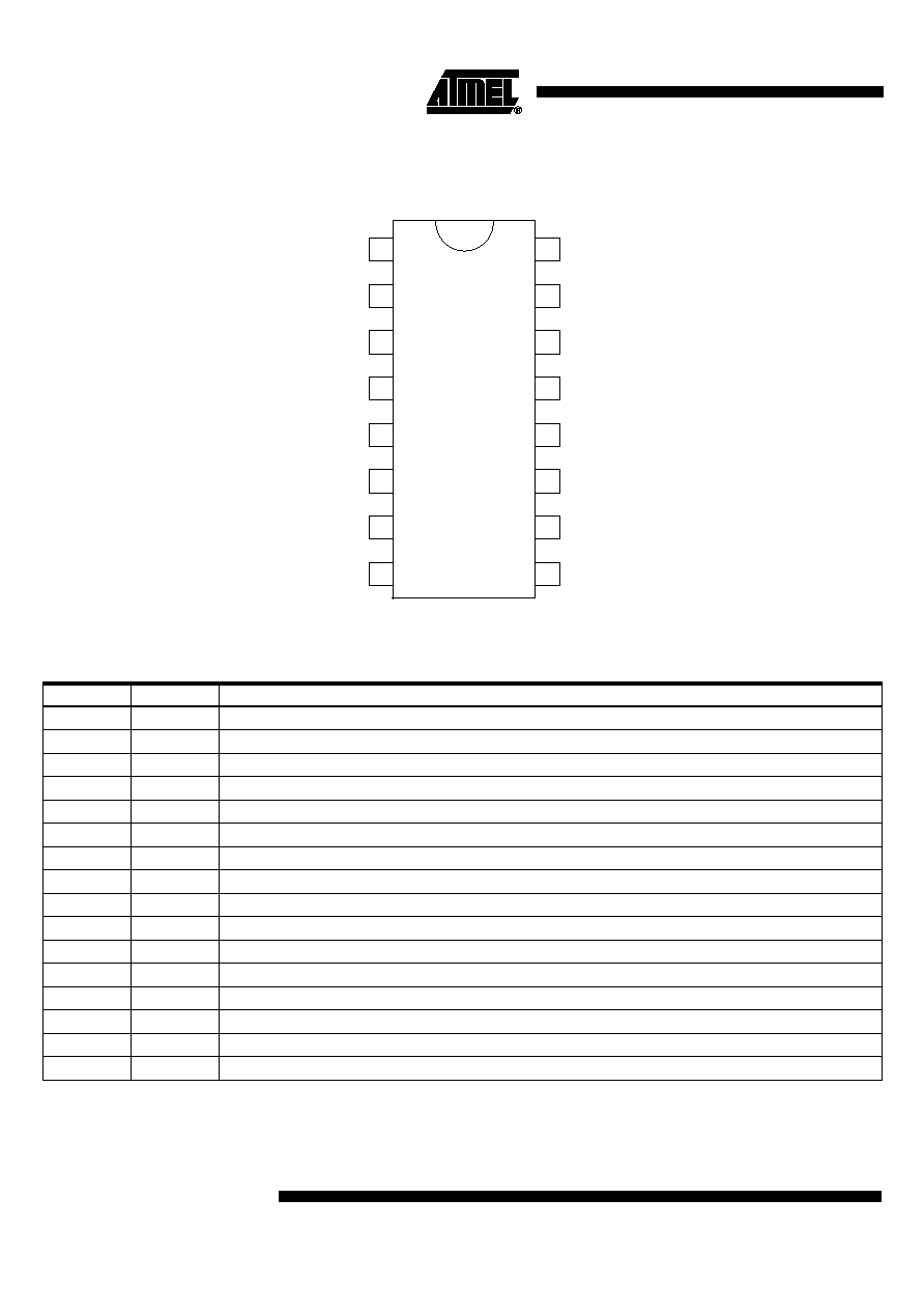
Pin Configuration
Figure 2. Pinning SO16
1
2
3
4
5
6
7
8
16
15
14
13
12
11
10
9
FMGAIN
AGC
VREF2
NC
GND2
AMIN
FMIN
GND1
VS
AGCADJ
VREF1
AMOUT1
AMOUT
NC
NC
FMOUT
Pin Description
Pin
Symbol
Function
1
FMIN
FM input
2
GND1
Ground for FM part
3
FMGAIN
FM gain adjustment
4
AGC
AGC output
5
VREF2
Reference voltage 2 output
6
NC
Not connected
7
GND2
Ground for AM part
8
AMIN
AM input
9
NC
Not connected
10
AMOUT
AM output
11
AMOUT1
AM output
12
VREF1
Reference voltage 1 output
13
AGCADJ
Adjustment FM wide-band AGC threshold
14
VS
Supply voltage
15
FMOUT
FM output
16
NC
Not connected
3
U4254BM-M
4772B≠AUDR≠11/03
Pin Description
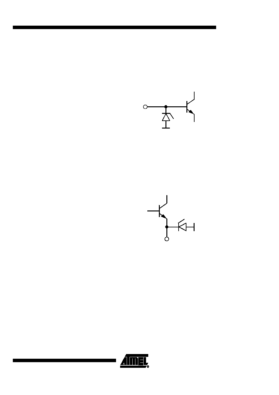
FMIN
FMIN, a bipolar transitor's base is the input of the FM amplifier. A resistor or a coil is
connected between FMIN and VREF2. If a coil is used, the noise performance is
excellent.
Figure 3. Internal Circuit at Pin FMIN
GND1
To avoid cross-talk between AM and FM signals, the circuit has two separate ground
pins. GND1 is the ground for the FM part.
FMGAIN
The DC current of the FM amplifier transistor is adjusted by an external resistor which is
connected between FMGAIN and GND1. To influence the AC gain of the amplifier, a
resistor is connected in series to a capacitor between FMGAIN and GND1. The capaci-
tor has to shorten frequencies of 100 MHz.
Figure 4. Internal Circuit at pin FMGAIN
AGC
DC current flows into the AGC pin at high FM antenna input signals. This current has to
be amplified via the current gain of an external PNP transistor that feeds a PIN diode.
This diode dampens the antenna's input signal and protects the amplifier input against
overload. The maximum current which flows in the AGC pin is approximately 1 mA. In
low-end applications, the AGC function is not necessary and the external components
can therefore be omitted.
ESD
1
FMIN
ESD
3
FMGAIN

4
U4254BM-M
4772B≠AUDR≠11/03
Figure 5. Internal Circuit at Pin AGC
AGCADJ
The threshold of the AGC can be adjusted by varying the DC current at pin AGCADJ. If
pin AGCADJ is connected directly to GND1, the threshold is set to 96 dBµV at the FM
amplifier output. If a resistor is connected between AGCADJ and GND1, the threshold is
shifted to higher values with increasing resistances. If AGCADJ is open, the threshold is
set to 106 dBµV.
Figure 6. Internal Circuit at Pin AGCADJ
FMOUT
The FM amplifier output is an open collector of a bipolar RF transistor. It should be con-
nected to V
S
via a coil.
Figure 7. Internal Circuit at Pin FMOUT
ESD
4
V
S
AGC
ESD
13
65 k
AGCADJ
ESD
15
FMOUT

5
U4254BM-M
4772B≠AUDR≠11/03
AMIN
The AM input has an internal bias voltage. The DC voltage at this pin is V
Ref1/2
. The input
resistance is about 470 k
. The input capacitance is less than 10 pF.
Figure 8. Internal Circuit at Pin AMIN
AMOUT, AMOUT1
The buffered AM amplifier consists of a complementary pair of CMOS source followers.
The transistor gates are connected to AMIN. The pin AMOUT is the NMOS transistor's
source, pin AMOUT1 is the PMOS transistor's source. Due to the two different DC levels
of these pins, they have to be connected together via an external capacitor of about
100 nF. By means of this technique an excellent dynamic range can be achieved.
Figure 9. Internal Circuit at Pins AMOUT1 and AMOUT
VREF1
VREF1 is the stabilized voltage for the AM amplifier and the AGC block. To achieve
excellent noise performance at LW frequencies, it is recommended that this pin be con-
nected to ground via an external capacitor of about 1 µF.
ESD
8
470 k
VREF1/2
AMIN
AMOUT1
ESD
ESD
AMOUT
11
10