 | –≠–ª–µ–∫—Ç—Ä–æ–Ω–Ω—ã–π –∫–æ–º–ø–æ–Ω–µ–Ω—Ç: U4468B | –°–∫–∞—á–∞—Ç—å:  PDF PDF  ZIP ZIP |
Rev. 4777A≠TVVCR≠01/04
Features
∑
5-V Supply Voltage
∑
Gain-controlled 3-stage Wide-band IF Amplifier
∑
Active Carrier Generation by FPLL Principle (Frequency-Phase-Locked-Loop) for True
Quadrature Demodulation
∑
Complete Alignment-free AM Demodulator
∑
Switchable Amplitude Detector for Gain Control, which Operates as a Peak Detector for
FM Sound and as a Mean Level Detector for AM Sound
Description
The U4468B is an integrated bipolar circuit for full multistandard sound IF signal pro-
cessing in TV/VTR and multimedia applications. It supplies AM signals as well as
FM/NICAM sound IF signals and thus allows the design of a universal sound IF mod-
ule for various applications.
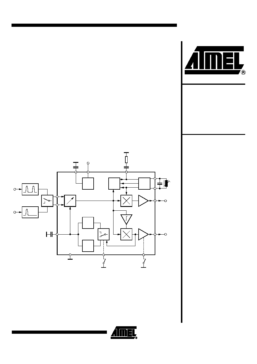
Figure 1. Block Diagram
Mean
FPLL
VCO
8
9
12
AM-det
6
Peak
level
IF-amp
2
1
REF
14
4
V
S
5
Loop
filter
VCO
7
13
10
3
IF AGC
Mean/peak
S
1
S
2
Mute
Intercarrier
(FM)
AF (AM)
AGC
IF
FM
IF
AM
905
05
Quasi-split
Sound Circuit
and AM
Demodulator IC
U4468B

2
U4468B
4777A≠TVVCR≠01/04
Circuit Description
IF Amplifier and AGC
The symmetrical IF input signal from the external SAW filter is fed to the pins 1 and 2. In
case of FM/NICAM applications, a SAW filter with double band-pass characteristic is
required for the vision and sound carrier. In case of the L-standard, a band-pass filter
with the center frequency at the L-sound carrier is used.
The amplifier consists of three AC-coupled wide-band IF stages. Each differential ampli-
fier stage is gain controlled by the AGC (Automatic Gain Control) voltage, available at
pin 3. The output signal of the IF amplifier is then applied to the FPLL carrier generation,
to the mixer for FM/NICAM signals and to the AM demodulator.
The IF-AGC is derived from the average level of the AM carrier (L-standard) or from the
peak value of the FM carrier (e.g., B/G standard). It controls the three-stage wide-band
amplifier to provide a constant SIF signal to the AM demodulator or to the QSS (quasi-
split sound) mixer.
Standard Switch
If the standard switch (pin 7) is in position "low" (for AM sound), the AGC is operating as
an average level detector. In position "open" or "high" (for FM/NICAM sound), the AGC
acts as a peak value detector.
Internal Voltage
Stabilizer
The internal band gap reference voltage (4.25 V at pin 4) ensures constant perfor-
mance, independent of supply voltage and temperature.
FPLL, VCO
The FPLL (frequency-phase-locked loop) circuit consists of a frequency detector and a
phase detector to generate a control voltage for the VCO tuning. In locked mode, the
VCO is controlled by the phase detector while in unlocked mode, the frequency detector
is superimposed. The VCO operates with an external resonance circuit (L and C paral-
lel) and is controlled by integrated varicaps.
A practicable VCO alignment of the external coil is the adjustment of the loop filter volt-
age (pin 5) to 2.3 V. At this value, the capture and hold range are centered.
AM Demodulator
The alignment-free AM demodulator is realized by a synchronous detector. The modu-
lated IF signal from the wide-band IF amplifier output is multiplied in phase with the
limited SIF signal to remove the AM. Then, the resulting AF signal of the demodulator
output is fed to the output amplifier and to the AGC stage.
Quasi-Split-Sound (QSS)
Mixer
The QSS mixer is realized by a multiplier circuit. The IF signal (FM/NICAM) is converted
to the intercarrier frequency by means of a quadrature signal from the generated picture
carrier provided by the PLL. The intercarrier signal is fed via an output amplifier to
pin 12.
Mute Switch
The AM sound output (pin 6) can be muted by switching the pulling mute switch (pin 10)
to "low".
3
U4468B
4777A≠TVVCR≠01/04
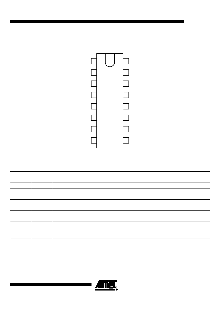
Pin Configuration
Figure 2. Pinning DIP16
1
2
3
4
5
6
7
8
16
15
14
13
12
11
10
9
U4468B
VIIF
VIIF
CAGC
CREF
LF
VO,AM
VSW,AGC
VVCO
VS
NC
NC
GND
VO,FM
NC
VSW,MUTE
VVCO
Pin Description
Pin
Symbol
Function
1, 2
VI,IF
IF input (symmetrical)
3
CAGC
Capacitor for the AGC time constant
4
CREF
Capacitor for the internal reference voltage
5
LF
Loop filter
6
VO,FM
AF output (AM sound)
7
VSW,AGC
Standard switch
8, 9
VVCO
VCO circuit
10
VSW,MUTE Mute switch
12
VO,FM
Intercarrier output (FM sound)
13
GND
Ground
14
VS
Supply voltage (5 V)
11, 15, 16
NC
Not connected
4
U4468B
4777A≠TVVCR≠01/04
Absolute Maximum Ratings
Stresses beyond those listed under "Absolute Maximum Ratings" may cause permanent damage to the device. This is a stress rating
only and functional operation of the device at these or any other conditions beyond those indicated in the operational sections of this
specification is not implied. Exposure to absolute maximum rating conditions for extended periods may affect device reliability.
Reference point pin 13, unless otherwise specified.
Parameters
Pin
Symbol
Value
Unit
Supply voltage range
14
V
s
4.5 to 9.0
V
Supply current
14
I
s
55
mA
Power dissipation (V
S
= 9 V)
P
500
mW
Output currents
6, 12
I
out
5
mA
External voltages
1 - 4, 6, 12
V
ext
+4.5
V
5, 8, 9
+3.5
V
7, 10
V
s
V
Junction temperature
T
j
+125
∞C
Operating temperature range
T
amb
0 to +85
∞C
Storage temperature
T
stg
-25 to +125
∞C
Electrostatic handling
(1)
All
V
ESD
±300
V
Note:
1. Equivalent to discharging a 200-pF capacitor through a 0-
W
resistor
Thermal Resistance
Parameters
Symbol
Value
Unit
Junction ambient when soldered to PCB
R
thJA
60
K/W
5
U4468B
4777A≠TVVCR≠01/04
Electrical Characteristics
V
S
= +5 V, T
amb
= +25∞C; reference point pin 13, unless otherwise specified.
Parameters
Test Conditions
Symbol
Min.
Typ.
Max.
Unit
DC Supply (Pin 14)
Supply voltage
V
S
4.5
5.0
9.0
V
Supply current
V
in
=10 mV or V
3
= 2 V
I
S
40
mA
IF Input (Pins 1, 2)
Minimum IF input signal
Output signal: -3 dB
v
in
50
µV
rms
Maximum IF input signal
Output signal: +1 dB
v
in
70
100
mV
rms
Input impedance
(1)
R
in
1.2
k
W
Input capacitance
(1)
C
in
2
pF
SIF-AGC (Pin 3)
IF gain control range
G
v
60
65
dB
AGC capacitor
C
AGC
4.7
µF
FPLL and VCO (Pins 5, 8, and 9)
Maximum oscillator frequency
For carrier generation
f
VCO
70
MHz
Vision carrier capture range
f
VCO
= 38.9 MHz
C
VCO
= 6.2 pF
D
f
cap
±1.5
±2
MHz
Oscillator drift (free running) as
function of temperature
D
T
amb
= 55
∞
C,
f
VCO
= 38.9 MHz
C
VCO
= 6.2 pF
(2)
D
f/
D
T
-0.3
%
Standard Switch (Pin 7)
Switching voltage for mode 1:
FM/NICAM sound
Peak value control
(3)
V
sw1
2.0
V
S
V
Switching voltage for mode 2:
AM sound
Average level control
V
sw2
0
1.5
V
Switching current
I
sw
±100
µA
AM Mute Switch (Pin 10)
Switching voltage
AM output active
V
mute1
open
Switching voltage
AM output switched off
V
mute2
0
1.5
V
Switching current
I
mute
-100
µA
Intercarrier Output (Pin 12)
(4)
DC output voltage
V
DC
2
V
Output resistance
(1)
R
out
200
W
Intercarrier output signal
v
in
= 10 mV
5.5 MHz output signal
V
out
100
150
mV
rms
Intercarrier bandwidth
-1 dB
-3 dB
B
TBD
TBD
MHz
MHz
Notes:
1. This parameter is given as an application information and is not tested during production.
2. The oscillator drift is related to the picture carrier frequency, with an external temperature-compensated LC circuit.
3. Without external control voltage (pin 7 open), the IC automatically operates in mode 1.
4. Picture carrier PC = 38.9 MHz; sound carrier SC
1
= 33.4 MHz, SC
2
= 33.16 MHz;
PC/SC
1
=13 dB; PC/SC
2
= 20 dB; PC unmodulated (equivalent to sync peak level).
5. Sound carrier SC = 32.4 MHz, modulated with f
mod
= 1 kHz, m = 54%; v
in
= 10 mV.