1
Features
∑
Six High-side and Six Low-side Drivers
∑
Outputs Freely Configurable as Switch, Half Bridge or H-bridge
∑
Capable to Switch All Kinds of Loads Such as DC Motors, Bulbs, Resistors, Capacitors
and Inductors
∑
0.6 A Continuous Current Per Switch
∑
Low-side: R
DSon
< 1.5
Versus Total Temperature Range
∑
High-side: R
DSon
< 2.0
Versus Total Temperature Range
∑
Very Low Quiescent Current I
S
< 20 µA in Standby Mode
∑
Outputs Short-circuit Protected
∑
Overtemperature Prewarning and Protection
∑
Under- and Overvoltage Protection
∑
Various Diagnosis Functions Such as Shorted Output, Open Load, Overtemperature
and Power Supply Fail
∑
Serial Data Interface
∑
Daisy Chaining Possible
∑
SO28 Power Package
Description
The U6815BM is a fully protected driver interface designed in 0.8-µm BCDMOS tech-
nology. It is used to control up to 12 different loads by a microcontroller in automotive
and industrial applications.
Each of the 6 high-side and 6 low-side drivers is capable to drive currents up to
600 mA. The drivers are freely configurable and can be controlled separately from a
standard serial data interface. Therefore, all kinds of loads such as bulbs, resistors,
capacitors and inductors can be combined. The IC design especially supports the
applications of H-bridges to drive DC motors.
Protection is guaranteed in terms of short-circuit conditions, overtemperature, under-
and overvoltage. Various diagnostic functions and a very low quiescent current in
standby mode enable a wide range of applications. Automotive qualification referring
to conducted interferences, EMC protection and 2-kV ESD protection gives added
value and enhanced quality for the strict automotive requirements.
Dual Hex DMOS
Output Driver
with Serial Input
Control
U6815BM
Rev. 4545B≠BCD≠12/02
2
U6815BM
4545B≠BCD≠12/02
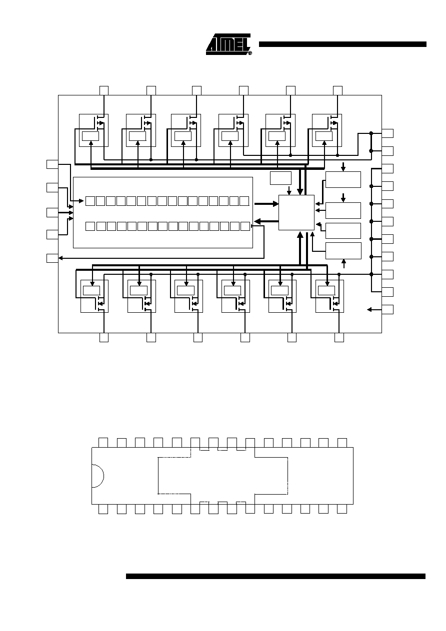
Figure 1. Block Diagram
Pin Configuration
Figure 2. Pinning SO28
CLK
CS
INH
DO
DI
HS1
HS2
HS3
HS4
HS5
HS6
13
15
3
2
28
OV -
protection
Osc
Fault
Detect
O
H
S
V
S
V
S
GND
GND
GND
GND
GND
GND
GND
GND
Vcc
LS6
LS1
LS2
LS3
LS4
LS5
Control
logic
V
S
Vcc
Fault
Detect
Fault
Detect
Fault
Detect
Fault
Detect
Fault
Detect
Fault
Detect
Fault
Detect
S
T
C
S
I
L
D
S
6
H
S
5
L
S
6
L
S
5
H
S
4
L
S
4
H
S
3
L
S
3
H
S
2
L
S
2
H
S
1
L
S
1
R
R
P
S
F
I
N
H
S
C
D
H
S
6
H
S
5
L
S
6
L
S
5
H
S
4
L
S
4
H
S
3
L
S
3
H
S
2
L
S
2
H
S
1
L
S
1
T
P
Input Register
Output Register
16
14
11
4
1
27
19
10
5
6
7
8
9
20
21
22
23
Fault
Detect
Fault
Detect
Fault
Detect
Fault
Detect
26
25
24
17
18
UV -
protection
V
S
Vcc
P - ON -
Reset
Thermal
protection
15
13
12
3
2
28
1
2
3
4
5
6
7
8
10
9
27
22
21
20
18
19
17
12
11
28
25
26
23
24
LS4
16
15
14
13
HS6
LS6
DI
CLK
CS
GND VCC DO
INH
LS1
HS1
LS5 HS5
HS4
VS
VS
LS3
HS3 HS2
LS2
GND GND GND
GND
GND GND GND
Lead frame
U6815BM
3
U6815BM
4545B≠BCD≠12/02
Pin Description
Pin
Symbol
Function
1
LS5
Low-side driver output 5, power-MOS open drain with internal reverse diode, overvoltage protection by
active zenering, short-circuit protection, diagnosis for short and open load
2
HS5
High-side driver output 5, power-MOS open drain with internal reverse diode, overvoltage protection by
active zenering, short-circuit protection, diagnosis for short and open load
3
HS4
High-side driver output 4 (see Pin 2)
4
LS4
Low-side driver output 4 (see Pin 1)
5
VS
Power supply output stages HS4, HS5, HS6, internal supply; external connection to Pin 10 necessary
6, 7, 8, 9
GND
Ground, reference potential, internal connection to Pin 20 - 23, cooling tab
10
VS
Power supply output stages HS1, HS2 and HS3
11
LS3
Low-side driver output 3 (see Pin 1)
12
HS3
High-side driver output 3 (see Pin 2)
13
HS2
High-side driver output 2 (see Pin 2)
14
LS2
Low-side driver output 2 (see Pin 1)
15
HS1
High-side driver output 1 (see Pin 2)
16
LS1
Low-side driver output 1 (see Pin 1)
17
INH
Inhibit input, 5-V logic input with internal pull down, low = standby, high = normal operating
18
DO
Serial data output, 5-V CMOS logic level tristate output for output (status) register data, sends 16-bit
status information to the microcontroller (LSB is transferred first).
Output will remain tristated unless device is selected by CS = low, therefore, several ICs can operate
on one data output line only.
19
VCC
Logic supply voltage (5 V)
20, 21, 22, 23
GND
Ground (see Pins 6 - 9)
24
CS
Chip select input, 5-V CMOS logic level input with internal pull up, low = serial communication is
enabled, high = disabled
25
CLK
Serial clock input, 5-V CMOS logic level input with internal pull down, controls serial data input
interface and internal shift register (f
max
= 2 MHz)
26
DI
Serial data input, 5-V CMOS logic level input with internal pull down, receives serial data from the
control device, DI expects a 16-bit control word with LSB being transferred first
27
LS6
Low-side driver output 6 (see Pin 1)
28
HS6
High-side driver output 6 (see Pin 2)
4
U6815BM
4545B≠BCD≠12/02
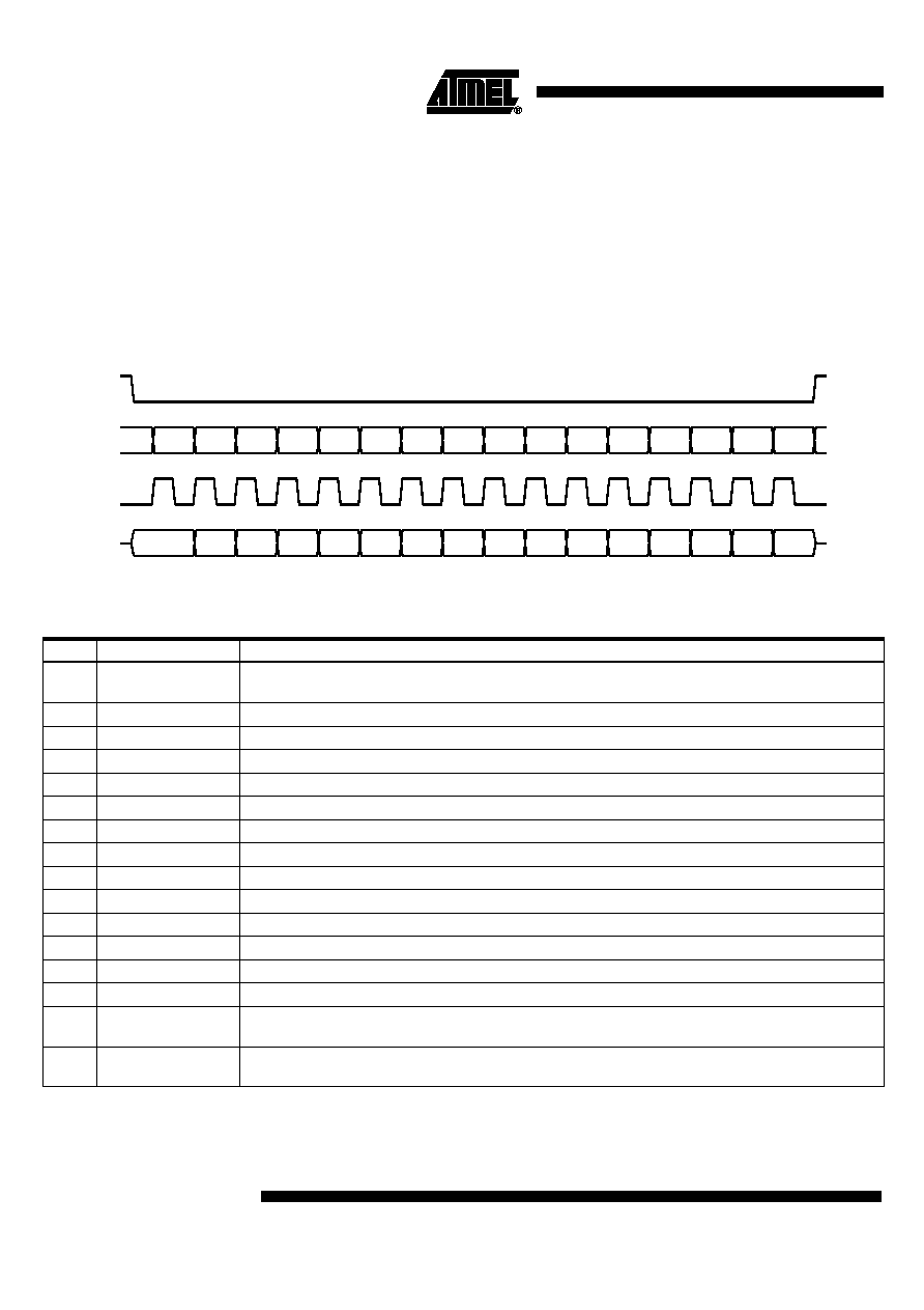
Functional Description
Serial Interface
Data transfer starts with the falling edge of the CS signal. Data must appear at DI syn-
chronized to CLK and are accepted on the falling edge of the CLK signal. LSB (bit 0,
SRR) has to be transferred first. Execution of new input data is enabled on the rising
edge of the CS signal. When CS is high, Pin DO is in tristate condition. This output is
enabled on the falling edge of CS. Output data will change their state with the rising
edge of CLK and stay stable until the next rising edge of CLK appears. LSB (bit 0, TP) is
transferred first.
Figure 3.
Data Transfer
Input Data Protocol
SRR
LS1
HS1
LS2
HS2
LS3
HS3
LS4
HS4
LS5
HS5
LS6
HS6
OLD
SCT
SI
CS
DI
CLK
DO
TP
SLS1 SHS1 SLS2 SHS2 SLS3 SHS3 SLS4 SHS4 SLS5
SHS5 SLS6 SHS6
SCD
INH
PSF
0
1
2
3
4
5
6
7
8
9
10
11
12
13
14
15
Bit
Input Register
Function
0
SRR
Status register reset (high = reset; the bits PSF, SCD and overtemperature shutdown in the output
data register are set to low)
1
LS1
Controls output LS1 (high = switch output LS1 on)
2
HS1
Controls output HS1 (high = switch output HS1 on)
3
LS2
See LS1
4
HS2
See HS1
5
LS3
See LS1
6
HS3
See HS1
7
LS4
See LS1
8
HS4
See HS1
9
LS5
See LS1
10
HS5
See HS1
11
LS6
See LS1
12
HS6
See HS1
13
OLD
Open load detection (low = on)
14
SCT
Programmable time delay for short circuit and overvoltage shutdown (short circuit shutdown delay
high/low = 100 ms/12.5 ms, overvoltage shutdown delay high/low = 15 ms/3.5 ms
15
SI
Software inhibit; low = standby, high = normal operation
(data transfer is not affected by standby function because the digital part is still powered)
5
U6815BM
4545B≠BCD≠12/02
After power-on reset, the input register has the following status:
Output Data Protocol
Note:
1. Bit 0 to 15 = high: overtemperature shutdown
Power Supply Fail
In case of over-/undervoltage at Pin VS, an internal timer is started. When the overvolt-
age delay time (t
dOV
) programmed by the SCT Bit, or the undervoltage delay time (t
dUV
)
is reached, the power supply fail bit (PSF) in the output register is set and all outputs are
disabled. When normal voltage is present again, the outputs are enabled immediately.
The PSF bit remains high until it is reset by the SRR bit in the input register.
Open-load Detection
If the open-load detection bit (OLD) is set to low, a pull-up current for each high-side
switch and a pull-down current for each low-side switch is turned on (open-load detec-
tion current I
HS1-6
, I
LS1-6
). If V
VS
-V
HS1-6
or V
LS1-6
is lower than the open-load detection
threshold (open-load condition) the corresponding bit of the output in the output register
is set to high. Switching on an output stage with OLD bit set to low disables the open-
load function for this output.
Bit 15
(SI)
Bit 14
(SCT)
Bit 13
(OLD)
Bit 12
(HS6)
Bit 11
(LS6)
Bit 10
(HS5)
Bit 9
(LS5)
Bit 8
(HS4)
Bit 7
(LS4)
Bit 6
(HS3)
Bit 5
(LS3)
Bit 4
(HS2)
Bit 3
(LS2)
Bit 2
(HS1)
Bit 1
(LS1)
Bit 0
(SRR)
H
H
H
L
L
L
L
L
L
L
L
L
L
L
L
L
Bit
Output (Status) Register
Function
0
TP
Temperature prewarning: high = warning (overtemperature shut down)
(1)
1
Status LS1
Normal operation: high = output is on, low = output is off
Open-load detection: high = open load, low = no open load (correct load condition is detected
if the corresponding output is switched off)
2
Status HS1
Normal operation: high = output is on, low = output is off
Open-load detection: high = open load, low = no open load (correct load condition is detected
if the corresponding output is switched off)
3
Status LS2
Description see LS1
4
Status HS2
Description see HS1
5
Status LS3
Description see LS1
6
Status HS3
Description see HS1
7
Status LS4
Description see LS1
8
Status HS4
Description see HS1
9
Status LS5
Description see LS1
10
Status HS5
Description see HS1
11
Status LS6
Description see LS1
12
Status HS6
Description see HS1
13
SCD
Short circuit detected: set high, when at least one output is switched off by a short circuit
condition
14
INH
Inhibit: this bit is controlled by software (bit SI in input register) and hardware inhibit (Pin 17).
High = standby, low = normal operation
15
PSF
Power supply fail: over- or undervoltage at Pin VS detected