 | –≠–ª–µ–∫—Ç—Ä–æ–Ω–Ω—ã–π –∫–æ–º–ø–æ–Ω–µ–Ω—Ç: UA1E | –°–∫–∞—á–∞—Ç—å:  PDF PDF  ZIP ZIP |

Rev. 4319B≠ULC≠12/03
1
Features
∑
High-performance ULC Family Suitable for Large-sized CPLDs and FPGAs
∑
From 46K Gates up to 780K Gates Supported
∑
From 18 Kbit to 390 Kbit DPRAM
∑
Compatible with Xilinx or Altera
∑
Pin-counts to Over 976 pins
∑
Any Pin≠out Matched
∑
Full Range of Packages: DIP, SOIC, LCC/PLCC, PQFP/TQFP, BGA, PGA/PPGA
∑
Low Quiescent Current: 0.3 nA/gate
∑
Available in Commercial and Industrial Grades
∑
0.35 µm Drawn CMOS, 3 and 4 Metal Layers
∑
Library Optimised for Synthesis, Floor Plan & Testability
Generation (ATPG)
∑
High Speed Performances:
≠ 150 ps Typical Gate Delay @3.3V
≠ Typical 600 MHz Toggle Frequency @3.3V
≠ Typical 360 MHz Toggle Frequency @2.5V
∑
High System Frequency Skew Control:
≠ Clock Tree Synthesis Software
∑
Low Power Consumption:
≠ 0.25
µ
W/Gate/ MHz @3.3V
≠ 0.18
µW
/Gate/ MHz @2.5V
∑
Power on Reset (Internal)
∑
Standard 2, 4, 6, 8,10, 12 and 18mA I/Os
∑
CMOS/TTL/PCI LVCMOS, LVTTL, GTL, HSTL, LVDS Interfaces
∑
ESD (2 kV) and Latch-up Protected I/O
∑
High Noise & EMC Immunity:
≠ I/O with Slew Rate Control
≠ Internal Decoupling
≠ Signal Filtering between Periphery & Core
∑
Thick oxide matrices allowing 5V Compliance
∑
Internal Regulator 5V -> 3.3V
∑
PLL 0.35µm with Integrated Filter
Description
The UA1E series of ULCs is well suited for conversion of large sized CPLDs and
FPGAs. We can support within one ULC from 18 Kbits to 390 Kbits DPRAM and from
46 Kgates to 780 Kgates. Typically, ULC die size is 50% smaller than the equivalent
FPGA die size. DPRAM blocks are compatible with Xilinx or Altera FPGA blocks.
Devices are implemented in high≠performance CMOS technology with 0.35µm
(drawn) channel lengths, and are capable of supporting flip≠flop toggle rates of 200
MHz at 3.3V and 180 MHz at 2.5V, and input to output delays as fast as 150ps at 3.3V.
The architecture of the UA1E series allows for efficient conversion of many PLD archi-
tecture and FPGA device types with higher IO count. A compact RAM cell, along with
the large number of available gates allows the implementation of RAM in FPGA archi-
tectures that support this feature, as well as JTAG boundary≠scan and scan≠path
testing.
Conversion to the UA1E series of ULC can provide a significant reduction in operating
power when compared to the original PLD or FPGA. This is especially true when com-
pared to many PLD and CPLD architecture devices, which typically consume 100mA
or more even when not being clocked. The UA1E series has a very low standby con-
sumption of 0.3nA/gate typically commercial temperature, which would yield a
standby current of 42µA on a 144,000 gates design. Operating consumption is a strict
0.35
µm
ULC
Series with
Embedded
DPRAM
UA1E

2
4319B≠ULC≠12/03
function of clock frequency, which typically results in a power reduction of 50% to 90%
depending on the device being compared.
The UA1E series provides several options for output buffers, including a variety of drive
levels up to 18mA. Schmitt trigger inputs are also an option. A number of techniques are
used for improved noise immunity and reduced EMC emissions, including: several inde-
pendent power supply busses and internal decoupling for isolation; slew rate limited
outputs are also available if required.
The UA1E series is designed to allow conversion of high performance 3.3V devices as
well as 2.5V devices. Support of mixed supply conversions is also possible, allowing
optimal trade≠offs between speed and power consumption.
Array Organization
Table 1. Matrices
Note:
1. Arrays with internal regulators 5V -> 3.3V and Power on Reset.
Part Number
Max Pads
KGates
DPRAM Kbits
PLL
USD700
700
780
390
4
USD594
594
590
230
3
USD492
492
520
243
2
USD432
432
374
144
2
USD384
384
300
99
0
USD312
312
150
72
0
USD256
256
124
48
2
USD228
228
98
38
2
USD210
210
95
18
2
USD170
(1)
170
67
0
0
USD134
(1)
134
33
0
0

3
4319B≠ULC≠12/03
Matrix Examples
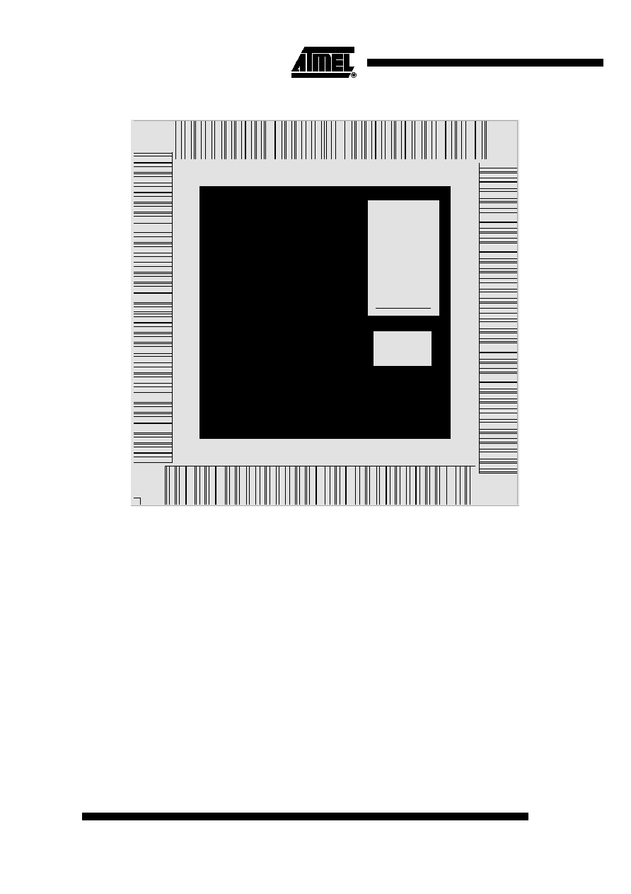
Figure 1. ATL35_M484E1 Matrix with 108 DPRAMS and 2 PLL's
PLL
DPRAM
PLL
4
4319B≠ULC≠12/03
Figure 2. ATL35_MI34E1 Matrix with 1 voltagte Regulator 5V - 3V and Power on Reset
Architecture
The basic element of the UA1E family is called a cell. One cell can typically implement
between one to four FPGA gates. Cells are located contiguously throughout the core of
the device, with routing resources provided in three to four metal layers above the cells.
Some cell blockage does occur due to routing, and utilization will be significantly greater
with three metal routing than two. The sizes listed in the Product Outline are estimated
usable amounts using three metal layers. I/O cells are provided at each pad, and may
be configured as inputs, outputs, I/Os, V
DD
or V
SS
as required to match any FPGA or
PLD pinout.
In order to improve noise immunity within the device, separate V
DD
and V
SS
busses are
provided for the internal cells and the I/O cells.
I/O buffer interfacing
I/O Flexibility
All I/O buffers may be configured as input, output, bi-directional, oscillator or supply. A
level translator could be located close to each buffer.
5V - 3V
Regulator
POR

5
4319B≠ULC≠12/03
I/O Options
Inputs
Each input can be programmed as TTL, CMOS, or Schmitt Trigger, with or without a pull
up or pull down resistor.
Fast Output Buffer
Fast output buffers are able to source or sink 2 to 18mA at 3.3V according to the chosen
option. 36mA achievable, using 2 pads.
Slew Rate Controlled Output
Buffer
In this mode, the p≠ and n≠output transistors commands are delayed, so that they are
never set "ON" simultaneously, resulting in a low switching current and low noise. These
buffers are dedicated to very high load drive.
2.5V Compatibility
The UA1E series of ULC's is fully capable of supporting high≠performance operation at
2.5V or 3.3V. The performance specifications of any given ULC design however, must
be explicitly specified as 2.5V, 3.3V or both.
Power Supply and Noise
Protection
In order to improve the noise immunity of the UA1E core matrix, several mechanisms
have been implemented inside the UA1E arrays. Two types of protection have been
added: one to limit the I/O buffer switching noise and the other to protect the I/O buffers
against the switching noise coming from the matrix.
The speed and density of the UA1E technology cause large switching current spikes, for
example when:
∑
16 high current output buffers switch simultaneously, or
∑
10% of the 700 000 gates are switching within a window of 1ns.
Sharp edges and high currents cause some parasitic elements in the packaging to
become significant. In this frequency range, the package inductance and series resis-
tance should be taken into account. It is known that an inductor slows down the setting
time of the current and causes voltage drops on the power supply lines. These drops
can affect the behavior of the circuit itself or disturb the external application (ground
bounce).
I/O Buffers Switching Protection
Three features are implemented to limit the noise generated by the switching current:
∑
The power supplies of the input and output buffers are separated.
∑
The rise and fall times of the output buffers can be controlled by an internal
regulator.
∑
A design rule concerning the number of buffers connected on the same power
supply line has been imposed.
Matrix Switching Current
Protection
This noise disturbance is caused by a large number of gates switching simultaneously.
To allow this without impacting the functionality of the circuit, three new features have
been added:
∑
Decoupling capacitors are integrated directly on the silicon to reduce the power
supply drop.
∑
A power supply network has been implemented in the matrix. This solution reduces
the number of parasitic elements such as inductance and resistance and constitutes
an artificial V
DD
and Ground plane. One mesh of the network supplies approximately
150 cells.
∑
A low pass filter has been added between the matrix and the input to the output
buffer. This limits the transmission of the noise coming from the ground or the V
DD
supply of the matrix to the external world via the output buffers.