 | –≠–ª–µ–∫—Ç—Ä–æ–Ω–Ω—ã–π –∫–æ–º–ø–æ–Ω–µ–Ω—Ç: A431A | –°–∫–∞—á–∞—Ç—å:  PDF PDF  ZIP ZIP |

KSD-I0A003-000
1
A431x
Programmable Voltage Reference
Description
The A431 series are 3-terminal precision shunt regulators that are programmable over a wide voltage range of
2.495V to 16V with ±0.5%, ±1.0% tolerance. The A431 series have a low dynamic impedance of 0.15. These
features make the A431 series an excellent replacement for zener diodes in numerous applications circuits that
require a precision reference voltage.
Features
∑ Programmable output voltage from 2.495V to 16V
∑ Voltage reference tolerance : ±0.5%, ±1.0%
∑ Cathode current capability of 1mA to 100mA
Ordering
Information
Type NO.
Marking
Package Code
A431x
A431
TO-92
: Grade => A:±1% , B:±0.5%
Outline Dimensions
( Unit : mm )
4.
40~4.
80
4.40~4.80
0.50 Max.
13.
50~14.
50
3.
40~3.
60
0.
45 Max.
1.27 Typ.
1.27 Typ.
1 2 3
S
S
e
e
m
m
i
i
c
c
o
o
n
n
d
d
u
u
c
c
t
t
o
o
r
r
Symbol
PIN Connections
1. Reference
2. Anode
3. Cathode
Functional block diagram
=2.495V
V
REF
Reference(R)
Cathode(K)
+
-
Anode(A)

KSD-I0A003-000
2
A431x
Absolute maximum ratings
[Ta=25]
Characteristic
Symbol Rating
Unit
Cathode to Anode voltage
V
KA
18
V
Cathode current
I
K
150
mA
Reference input current
I
ref
10
mA
Power Dissipation
P
D
625
mW
Junction Temperature
T
J
150
Operating temperature range
T
opr
-40 ~ +85
Storage temperature range
T
stg
-55 ~ +150
Recommended operating conditions
Rating
Characteristic Symbol
Min. Max.
Unit
Cathode to Anode voltage
V
KA
V
ref
16 V
Cathode current
I
K
1
100
mA
Electrical Characteristics
(Ta=25 , unless otherwise noted.)
Characteristic Symbol
Condition
Min.
Typ.
Max. Unit
A431B 2.482
2.508
Reference voltage (Fig.1)
V
ref
V
KA
=V
ref
, I
K
=10mA
A431A 2.470
2.495
2.520
V
Reference input voltage
deviation over temperature
(Fig.1, Note1,2)
V
ref
V
KA
=V
ref
, I
K
=10mA
@ 0∞C Ta 70∞C
- 7 30
mV
V
ref
V
ref
=V
ref(16V)
-V
ref
Ratio of delta reference input
voltage to delta cathode
voltage (Fig.2)
V
KA
I
K
=10mA
V
ref
V
KA
16V
V
KA
=V
KA(16V)
-V
ref
- -1.0 -2.7
mV/V
Reference current (Fig.2)
I
ref
I
K
=10mA
R1=10K
, R2=
- 1.8 4.0 µ
Reference input current
deviation over temperature
(Fig.2, Note 1,2)
I
ref
I
K
=10mA
R1=10K
, R2=
@ 0∞C Ta 70∞C
- 0.4 2.5 µ
Minimum cathode current
for regulation
I
K(MIN)
V
KA
=V
ref
-
0.35
1.0
m
Off-state cathode current
(Fig.3)
I
K(off)
V
KA
=16V, V
ref
=0V -
2.7
1000
nA
Dynamic impedance
(Fig.1, Note3)
Z
KA
V
KA
=V
ref
, f
1.0KHz
1.0mA I
K
100mA
- 0.15 0.5

KSD-I0A003-000
3
A431x
1
ref
2
1
ref
KA
R
◊
I
+
)
R
R
+
1
(
◊
V
=
V
Note.
1. Ambient temperature range: T
LOW
= 0, T
High
= 70
2. The deviation parameters V
ref
and I
ref
are defined as the difference between the maximum value and minimum value
obtained over the full operating ambient temperature range that applied.
The average temperature coefficient of the reference input voltage,
ref
V
is defined as:
T
)
10
◊
)
25
=
T
(
V
V
(
=
)
ppm
(
V
a
6
a
ref
ref
ref
ref
V
can be positive or negative depending on whether V
ref
Min or V
ref
Max occurs at the lower ambient temperature, refer to
Fig. 8
Example : V
ref
= 30mV and the slope is positive,
V
ref
@ 25 = 2.495V
Ta = 70
3. The dynamic impedance Z
KA
is defined as:
K
KA
KA
I
V
=
When the device is operating with two external resistors, R1 and R2, (refer to Fig.2) the total dynamic impedance of the circuit
is given by:
)
R
R
+
1
(
◊
=
2
1
KA
'
KA
Fig. 1 Test circuit for V
KA
=V
ref
Fig. 2 Test circuit for V
KA
>V
ref
Fig. 3 Test circuit for I
K(off)
KA
Input
R1
R2
V
I
K(off)
I
ref
V
ref
I
K
KA
V
Input
I
K
V
ref
= V
ref
Max ≠ V
ref
Min
Ta = T
2
≠ T
1
Ambient Temperature
KA
V
Input
/
ppm
171
=
70
10
◊
)
495
.
2
03
.
0
(
=
)
ppm
(
V
6
ref
KSD-I0A003-000
4
A431x
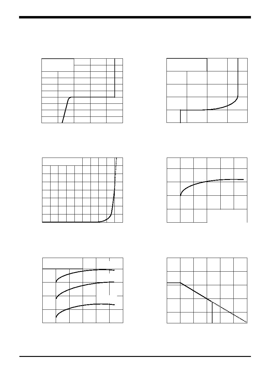
Electrical Characteristics Curves
(Continue)
3
Cath
od
e
cu
rr
e
n
t I
K
[mA]
0.0
0
1
2
4.0
1.0
-1
3.0
-0.2
2.0
Fig.4 I
K
vs V
KA
(1)
Fig.5 I
K
vs V
KA
(2)
Fig.6 I
K(off)
vs V
KA
100
3
25
-
100
2
Cathode c
u
rrent I
K
[
mA]
0
Cathode Voltage V
KA
[V]
1
-1
-2
-25
150
Cathode Voltage V
KA
[V]
Fig.7 V
ref
/V
KA
vs T
a
-75
-50
0
50
75
125
V
KA
=V
ref
Ta=25∞C
V
KA
=V
ref,
Ta=25∞C
I
Fig.8 V
ref
vs T
a
Fig.9 P
D
vs T
a
2.545
2.505
2.525
2.485
Ref
e
r
e
n
ce input v
o
ltag
e
V
ref
[V
]
2.465
Ambient Temperature T
a
[∞C]
2.445
Cathode Voltage V
KA
[V]
0.0
20
0.5
1.5
1.0
0
16
8
2.0
Of
f-state cathode c
u
rrent
I
K(of
f)
[µ
A
]
12
4
V
ref
=0V, Ta=25∞C
V
ref(min)
15
0
30
-15
75
60
45
V
KA
=V
ref ,
I
ref
=10mA
V
ref(typ)
V
ref(max)
45
15
0.0
0
-0.2
60
30
75
-0.1
-0.4
-0.3
-0.5
-15
Ratio o
f
de
lta
ref
e
renc
e inpu
t vo
lt
age
to d
e
lt
a
cathod
e voltag
V
ref
/
V
KA
[mV/V]
Ambient Temperature T
a
[∞C]
V
ref
V
KA
16V
I
K
=10mA
Ambient Temperature T
a
[∞C]
100
50
1000
25
600
125
75
150
800
200
400
0
Po
wer
di
ssi
pat
i
o
n
P
D
[m
W]
0

KSD-I0A003-000
5
A431x
Electrical Characteristics Curves
Unstable
Regions
V
KA
R
1
[K] R
2
[K]
A V
ref
0
B 10V 10 3.325
Fig.10 Pulse Response
7
10
4
-1
8
In
p
u
t
an
d
o
u
t
p
ut
v
o
l
t
a
ge
≠
V
4
t ≠ Time [s ]
6
2
0
2
0
1
3
5
6
Ta=25∞C
Fig.11 Test circuit for Fig. 10
Fig.14 Stability Boundary Conditions
I
K
Fig.15 Test circuit for Fig. 14
Input
Output
A
B
f=10KHz
GND
220
50
Output
Fig.12 Pulse Response (Magnify A of Fig.10)
Fig.13 Pulse Response (Magnify B of Fig.10)
7
5
4
-1
4
In
p
u
t
an
d
o
u
t
p
ut
v
o
l
t
a
ge
≠
V
2
t ≠ Time [s ]
3
1
0
2
0
1
3
5
6
7
5
4
-1
4
In
p
u
t
an
d
o
u
t
p
ut
v
o
l
t
a
ge
≠
V
2
t ≠ Time [s ]
3
1
0
2
0
1
3
5
6
Output
Input
Input
Output
Ta=25∞C
Ta=25∞C
R2
CL
0
GND
R1
Output