KSI-2052-001
1
S1117AD/S1117-xxD
Adjustable and Fixed LDO Voltage Regulator
Descriptions
The S1117A and S1117 series of positive adjustable and fixed regulators are designed to
provide 1A with higher efficiency than currently available devices. All internal circuitry is
designed to operate down to 1.3V input to output differential. On-Chip trimming adjusts
reference Voltage to 2%
Features
∑ Output Current of 1A
∑ 1.3V Maximum Dropout voltage at 1A Output Current
∑ 100% Thermal Limit Burn-In
∑ Fast Transient Response
Ordering Information
Type NO. Marking Package Code
S1117AD/S1117xxD S1117D D-PAK
:Voltage Code (Aj : 1.25V, 15:1.5V,:18: 1.8V, 25:2.5V, 285:2.85V, 33:3.3V, 50:5.0V)
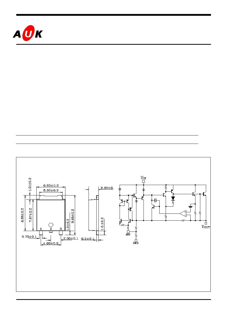
Outline Dimensions unit :
mm
S
S
e
e
m
m
i
i
c
c
o
o
n
n
d
d
u
u
c
c
t
t
o
o
r
r
PIN Connections
1. GND/ADJ
2. Output
3. Input
Block Diagram
KSI-2052-001
2
S1117AD/S1117-xxD
Absolute Maximum Ratings
Ta=25
∞C
Characteristic Symbol
Ratings
Unit
V
out
=1.25,1.5,1.8
16
Operating Input voltage
V
IN
V
out
= 2.5
2.8
3.3
5.0
20
V
Power Dissipation (without Heatsink)
P
D
1.3
W
Lead Temperature (Soldering, 10 sec)
T
LEAD
300 ∞C
Operating Junction Temperature
T
J
-30 ~ 125
∞C
Storage Temperature
T
STG
-55 ~ 150
∞C
Device Selection Guide (NOTE1
)
Electrical Characteristics
(Electrical Characteristics at T
J
= 25 and I
Load
=10mA unless otherwise specified.)
Characteristic Symbol
Device
Test
Condition
Min Typ Max
Unit
V
IN
= (V
out
+1.5V),I
OUT
= 10mA
1.238
1.262
S1117A
V
IN
= (V
out
+1.5V) to 12V
I
OUT
= 0 to 1000mA
* 1.225
1.25
1.275
V
IN
= (V
out
+1.5V),I
OUT
= 10mA
1.47
1.53
S1117-15
V
IN
= (V
out
+1.5V) to 12V
I
OUT
= 0 to 1000mA
* 1.44
1.5
1.56
V
IN
= (V
out
+1.5V),I
OUT
= 10mA
1.764
1.836
S1117-18
V
IN
= (V
out
+1.5V) to 12V
I
OUT
= 0 to 1000mA
* 1.728
1.8
1.872
V
IN
= (V
out
+1.5V),I
OUT
= 10mA
2.45
2.55
S1117-25
V
IN
= (V
out
+1.5V) to 12V
I
OUT
= 0 to 1000mA
* 2.4
2.5
2.6
V
IN
= (V
out
+1.5V),I
OUT
= 10mA
2.793 2.907
Output Voltage
V
OUT
S1117-285
V
IN
= (V
out
+1.5V) to 12V
I
OUT
= 0 to 1000mA
* 2.736
2.85
2.964
V
Device Output
Voltage
S1117A Adj
S1117-1.5 1.5V
S1117-1.8 1.8V
S1117-2.5 2.5V
S1117-2.85 2.85V
S1117-3.3 3.3V
S1117-5.0 5V
Note 1 : Other Fixed Versions are available Vout=1.5V to 5V

KSI-2052-001
3
S1117AD/S1117-xxD
Electrical Characteristics
(Continued)
(Electrical Characteristics at T
J
= 25 and I
LOAD
=10mA unless otherwise specified.)
Characteristic Symbol
Device
Test
Condition
Min Typ Max
Unit
V
IN
= (V
out
+1.5V),I
OUT
= 10mA
3.234
3.366
S1117-33
V
IN
= (V
out
+1.5V) to 12V
I
OUT
= 0 to 1000mA
* 3.168
3.3
3.432
V
IN
= (V
out
+1.5V),I
OUT
= 10mA
4.9
5.1
Output Voltage
V
OUT
S1117-50
V
IN
= (V
out
+1.5V) to 12V
I
OUT
= 0 to 1000mA
* 4.8
5.0
5.2
V
Line Regulation
Note1
V
OUT
All
(V
out
+1.5V) V
In
12V
I
OUT
=10mA
* - 10 30 mV
Load Regulation
Note1
V
OUT
All
(V
IN -
V
out
)=2V, 10mA
I
OUT
1A * - 10 30 mV
Quiescent
Current
I
Q
All Fixed
Versions V
IN
= 11.5V, I
OUT
=0mA *
-
3.6
10
mA
Minimum Load
Current
I
LMIN
S1117A
V
IN
=(V
OUT
+1.5), V
OUT
=0V *
3
7
mA
Adjust Pin Current
I
ADJ
S1117A
V
IN
= (V
out
+1.5V) to 12V
I
OUT
= 10mA
* 55 90 uA
Dropout Voltage
Note3
V
D
All
I
OUT
=1000mA
*
-
1.2
1.3
V
Ripple Rejection
Note2
RR All
V
IN
-V
OUT
=1.5V, f=120Hz
I
OUT
=1000mA, V
RIPPLE
=1V
P-P
60 72
-
dB
Output
Noise Voltage
eN
All
f=10 to 10KHz
-
100
-
uV
Output Current
I
OUT
All
(V
IN
-V
OUT
)=1.5V *
1
1.5
A
The * denotes the specifications which apply over the full temperature range.
Note 1: Low duty pulse testing with Kelvin connections required.
Note 2: 120Hz input ripple (C
ADJ
for ADJ=25uF)
Note 3: V
OUT
= 1%
Typical Applications
◊

KSI-2052-001
4
S1117AD/S1117-xxD
Electrical Characteristic Curves
Fig. 1 Minimum Load Current(Adjustable)
Fig. 2 Adjust Pin Current
Fig. 3 Temperature Stability
Fig. 4 Load Regulation
Fig. 5 Dropout Voltage
Fig. 6 Dropout Voltage - Temperature

KSI-2052-001
5
S1117AD/S1117-xxD
Electrical Characteristic Curves
.
Fig. 7 Load Transient Response
Fig. 8 Line Transient Response
Fig. 9 Ripple Rejection